Semiconductor integrated circuit device

一种集成电路、半导体的技术,应用在半导体器件、电路、半导体/固态器件制造等方向,能够解决改变布线、信号延迟时间不平衡、布局设计困难等问题

Inactive Publication Date: 2005-11-30
PANASONIC SEMICON SOLUTIONS CO LTD
View PDF1 Cites 2 Cited by
  • Summary
  • Abstract
  • Description
  • Claims
  • Application Information

AI Technical Summary

Problems solved by technology

In this way, depending on the arrangement direction (laying direction) of the wiring of each LSI wiring 204, 205, the delay time of the signal is unbalanced, and there is a problem that layout design is extremely difficult. Problems changing wiring
[0012] Furthermore, when the shielded wiring layer 215 itself is physically analyzed, there is a problem that the electrical connection of the shielded wiring layer 215 is clear at a glance.

Method used


Image

  • Semiconductor integrated circuit device
  • Semiconductor integrated circuit device
  • Semiconductor integrated circuit device

Examples


no. 1 Embodiment approach

[0044] Referring now to the drawings, a first embodiment of the present invention will be described.

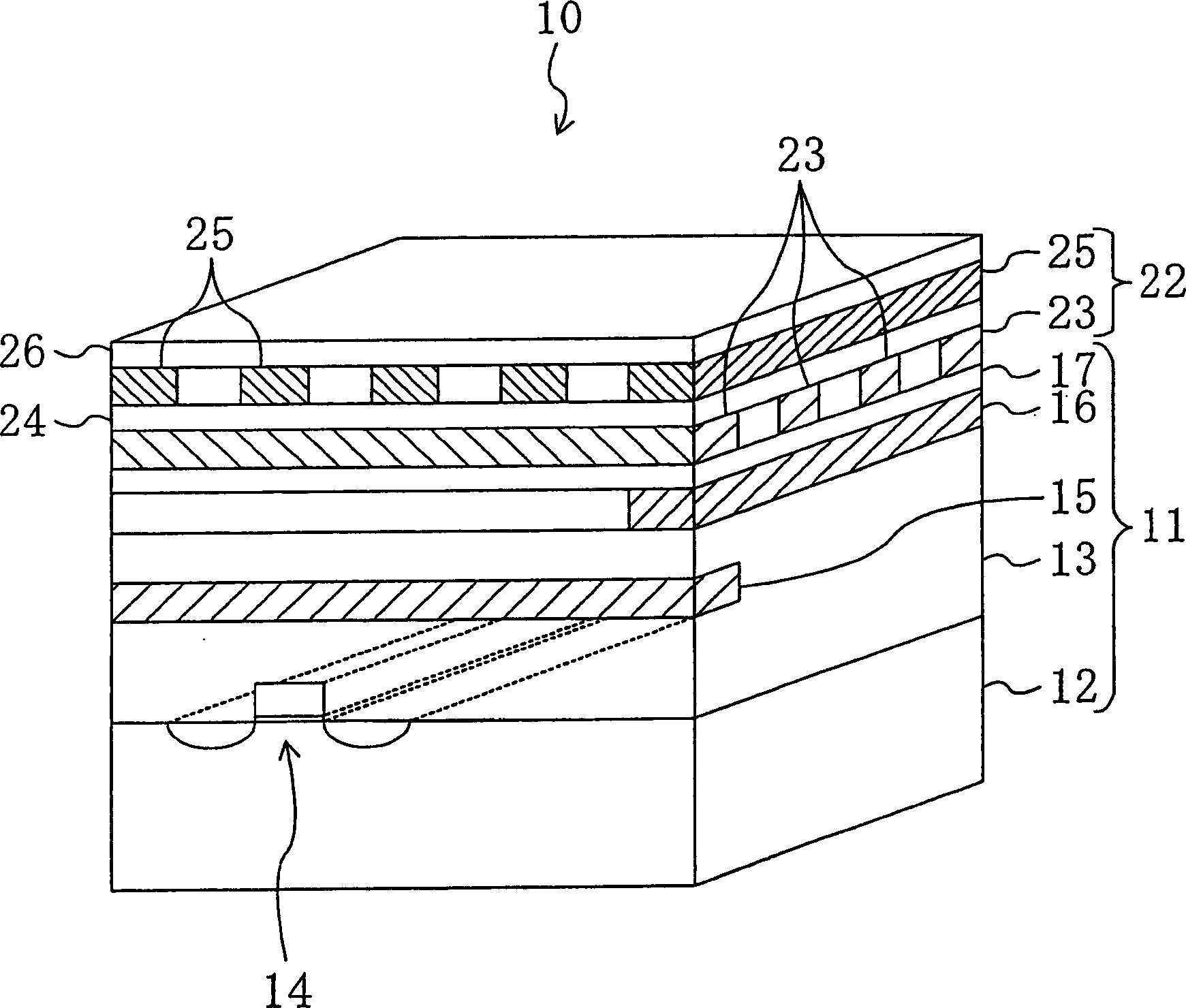
[0045] figure 1 It is a schematic diagram of the cross-sectional structure of the semiconductor integrated circuit device having the shielded wiring layer according to the first embodiment of the present invention.

[0046] as figure 1 As shown, the semiconductor integrated circuit device 10 according to the first embodiment is composed of an LSI function part 11 and a shield wiring layer 22 formed thereon.

[0047] The LSI function unit 11 is composed of a semiconductor substrate 12 and a first insulating film 13 , and a plurality of circuit elements including, for example, MOS transistors 14 are formed on the semiconductor substrate 12 . On the first insulating film 13, the first LSI wiring 15 and the second LSI wiring 16 are formed; on the first insulating film 13, the second insulating film 17 is formed.

[0048] The shield wiring layer 22 is composed of a lower shield...

no. 2 Embodiment approach

[0065] Next, a second embodiment of the present invention will be described with reference to the drawings.

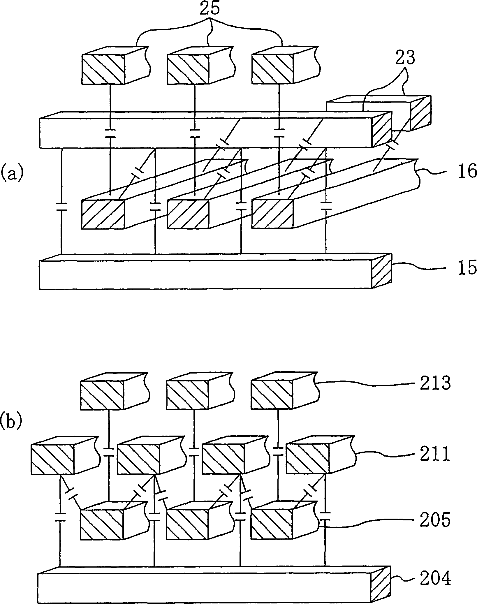
[0066] Figure 5 (a) and Figure 5 (b) is the semiconductor integrated circuit according to the second embodiment of the present invention, Figure 5 (a) shows the planar structure of the shielded wiring, Figure 5 (b) shows a partially enlarged planar structure of shield wiring and LSI wiring. exist Figure 5 (a) and Figure 5 In (b), for and figure 1 Structural components that are the same as those shown are assigned the same symbols, and description thereof will be omitted.

[0067] Such as Figure 5 As shown in (a), the shield wiring 52 according to the second embodiment is repeatedly arranged and extended parallel to one diagonal of the semiconductor integrated circuit device (chip) 10 having a planar square shape. Here, the shield wiring 52 may be one layer or two layers. In addition, when the upper shield wiring and the lower shield wiring are composed...

no. 3 Embodiment approach

[0077] Next, referring to the drawings, a third embodiment of the present invention will be described.

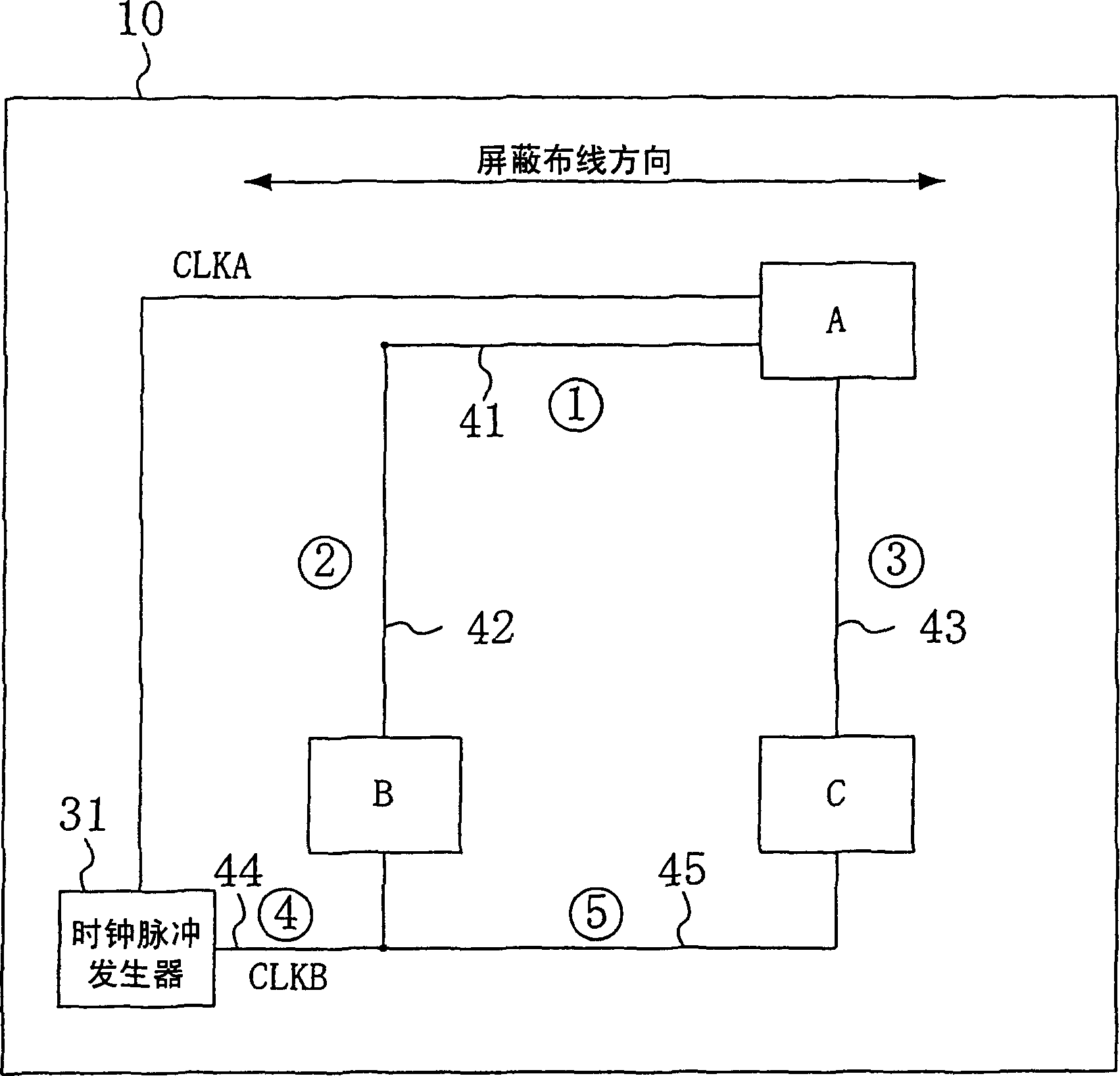
[0078] Figure 8 It is a schematic diagram showing an example of the switching circuit configuration of the shield wiring in the semiconductor integrated circuit device according to the third embodiment of the present invention.

[0079] Such as Figure 8 As shown, for example, one end or both ends of each of the eight shielded wirings 60a, 60b, . . .

[0080] The switching circuit 61 has an 8-bit register 65 connected to a setting signal line 66 which can be set externally, and a first switching circuit 64A, a second switching circuit 64A, and a second switching circuit 64A are respectively provided between the register 65 and the shielded wiring lines 60a to 60h. The switch circuit 64B, the third switch circuit 64C, and the fourth switch circuit 64D.

[0081] Although not shown in the figure, the register 65 has an 8-bit structure of bit 0 (b0), bit 1 (b1), . . . , bit...


PUM


Abstract

A semiconductor integrated circuit device (10) is composed of an LSI function unit (11) and a shield wiring layer (22) formed on the unit. The LSI function unit (11) includes a semiconductor substrate (12) and a first insulating film (13), and the semiconductor substrate (12) is formed with a circuit element including, for example, a MOS transistor (14). The shield wiring layer (22) is composed of a lower shield line (23), a third insulating film (24), an upper shield line (25), and a fourth insulating film (26) sequentially stacked above a second insulating film (17). The directions in which the lower and upper shield lines (23) and (25) are arranged intersect each other.

Description

technical field [0001] The present invention relates to a semiconductor integrated circuit device which requires high security such as an IC card and has means for preventing physical changes. Background technique [0002] In a semiconductor integrated circuit device (LSI) that requires high security, physical changes to circuits pose a serious threat, such as changes in the operation of the device and leakage of confidential information. [0003] For these changes, a focused ion beam (Focused Ion Beam: FIB) device is usually used to irradiate an ion beam to the upper part of the LSI. electrically connected. [0004] Below, refer to Figure 13 A prior art semiconductor integrated circuit device having shielded wiring is described. [0005] Such as Figure 13 As shown, on a semiconductor substrate 201, a MOS transistor 202 is formed; on this MOS transistor 202, a first insulating film 203 covering it is formed. In the first insulating film 203, a first LSI wiring 204 and a...

Claims


Application Information

Patent Timeline
Patent Type & Authority Applications(China)
IPC IPC(8): H01L23/522H01L23/528H01L23/58
CPCH01L2924/0002H01L23/576Y10S257/922H01L23/5225H01L23/5222H01L23/528H01L2924/00
Inventor 伊藤理惠松野则昭角田真人
Owner PANASONIC SEMICON SOLUTIONS CO LTD
Why Eureka
Try Eureka