Semiconductor device

a semiconductor and device technology, applied in the field of semiconductor devices, can solve the problems of reducing manufacturing efficiency, reducing production yield, and difficult to form optical waveguides and optical elements, so as to prevent a reduction of manufacturing efficiency, simplify the electrical wiring design, and increase manufacturing cost

Active Publication Date: 2015-05-19
SONY CORP +1
View PDF17 Cites 0 Cited by
  • Summary
  • Abstract
  • Description
  • Claims
  • Application Information

AI Technical Summary

Benefits of technology

[0012]However, in the optical signal transmission method in the chip, it is difficult to form an optical waveguide and an optical element at the same time in manufacture of a semiconductor chip in many cases, in consideration of design rules and conformity of used materials. Thus, an increase of manufacturing steps of a chip, and a reduction of a production yield rate are generated, and there is a case that the manufacture efficiency is reduced, and the manufacturing cost is increased. Also, to provide the optical element, an area on which other circuits are provided is reduced, and there is a case that the throughput of the chip is reduced.
[0016]In view of the foregoing issues, it is an object of the present invention to provide a semiconductor device capable of preventing a reduction of manufacture efficiency and an increase of a manufacturing cost, and simplifying an electrical wiring design, and capable of easily realizing improvement of a signal integrity, a size reduction of a device, and a reduction of a power consumption.
[0036]According to the embodiment of the present invention, it is possible to provide the semiconductor device capable of preventing a reduction of a manufacture efficiency and an increase of a manufacturing cost, and simplifying an electrical wiring design, and capable of easily realizing improvement of signal integrity, a size reduction of a device, a reduction of power consumption, and the like.

Problems solved by technology

However, in the optical signal transmission method in the chip, it is difficult to form an optical waveguide and an optical element at the same time in manufacture of a semiconductor chip in many cases, in consideration of design rules and conformity of used materials.
Thus, an increase of manufacturing steps of a chip, and a reduction of a production yield rate are generated, and there is a case that the manufacture efficiency is reduced, and the manufacturing cost is increased.
Because the distance of this electrical signal transmission is longer than at least the size of the LSI chip, the above-described problem is generated, and there is a case that the efficiency of the optical signal transmission is lost.
In particular, although superiority of the optical transmission to the electrical transmission is exhibited in the case where the transmission speed is high speed, the design of the above-described electrical transmission line is difficult in this case.
As described above, there is a case that it is difficult to use the optical signal transmission from a viewpoint of manufacture and performance, and it is difficult to sufficiently suppress the deterioration of the signal integrity such as the signal delay, the skew between the signals, the increase of the jitter, and the crosstalk between the wirings.
Also, due to the increase of the wiring length of the global wiring in a high-performance LSI, there is a case that a problem such as a size increase of a global wiring layer, an increase of an RC delay, and an increase of the power consumption accompanied by the size increase of the global wiring layer, and the increase of the RC delay are generated.

Method used


Image

  • Semiconductor device
  • Semiconductor device
  • Semiconductor device

Examples


first embodiment

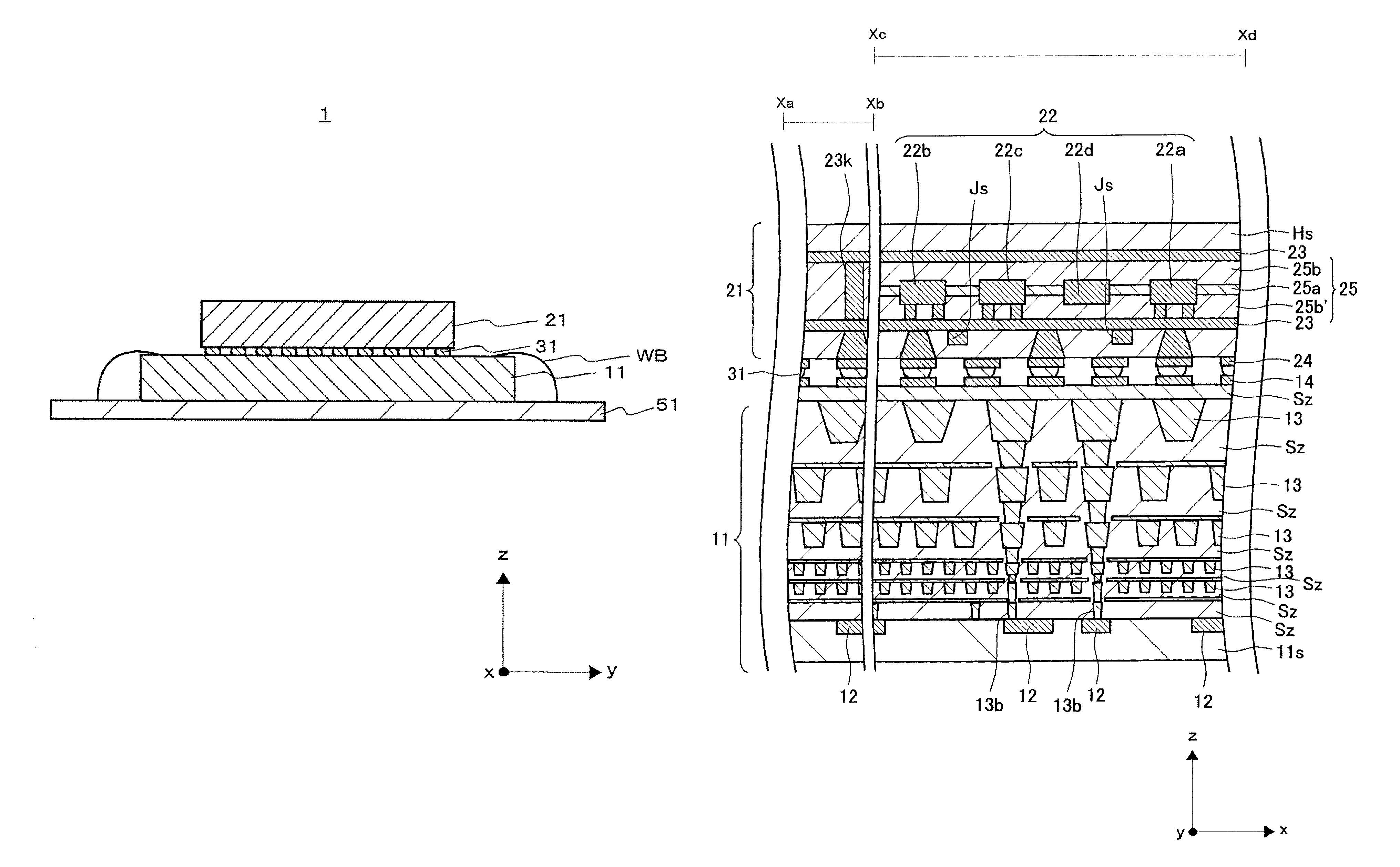
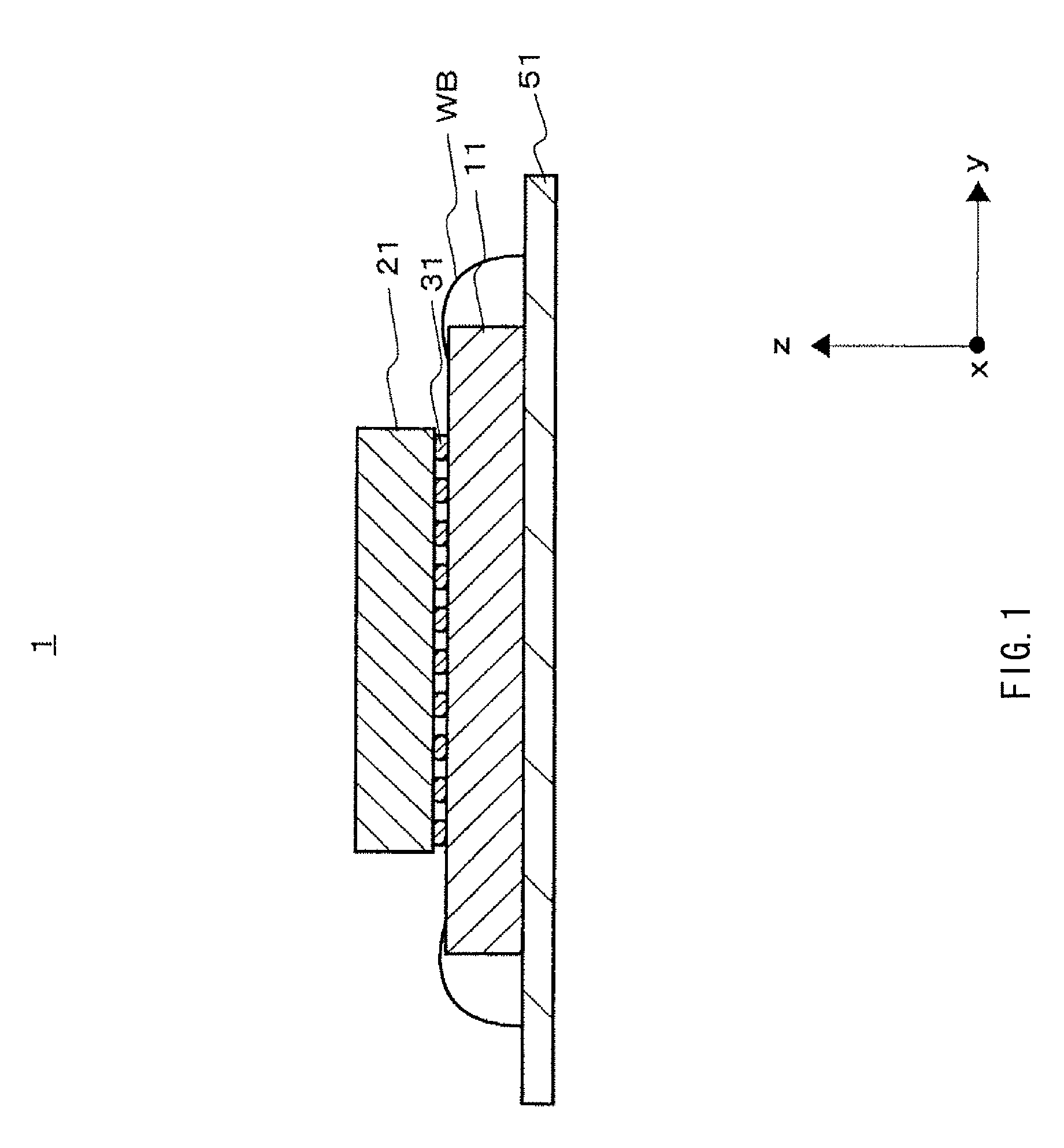
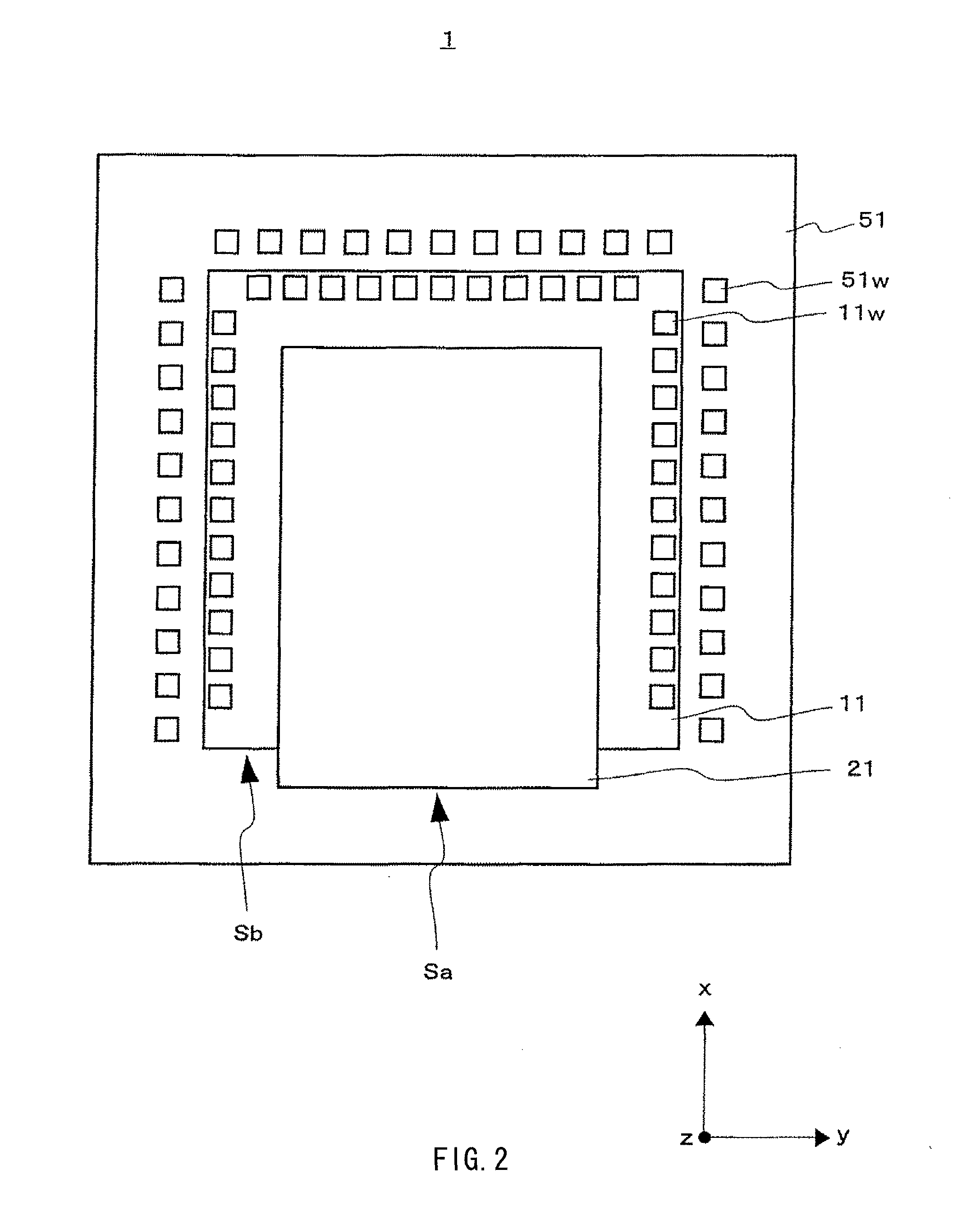
[0060]FIGS. 1 and 2 illustrate a configuration of a semiconductor device 1 according to the present invention, FIG. 1 illustrates its cross-sectional structure, and FIG.2 illustrates its plane configuration.

[0061]FIG.3 illustrates a cross-sectional configuration of a main part of the semiconductor device 1 in an enlarged manner, and, here, illustrates a cross section of an Xa-Xb part, and a cross section of an Xc-Xd part different from the Xa-Xb part. FIG. 4 illustrates a circuit configuration of the semiconductor device 1.

[0062]The semiconductor device 1 includes a semiconductor integrated circuit section 11, an optical wiring section 21, and a connection section 31.

[0063]Also, as illustrated in FIG. 4, the semiconductor device 1 includes a plurality of circuit blocks CB. The circuit block CB is constituted of, for example, a memory circuit CBm, a first calculation circuit CB1, and a second calculation circuit CB2. Although a detailed description will be given later, each of the me...

second embodiment

[0151]FIGS. 8 and 9 illustrate the configuration of the semiconductor device according to the present invention. FIG. 8 is a cross-sectional view of the semiconductor device 1, and FIG. 9 is a top face view of the semiconductor device 1. FIG. 8 illustrates a cross-section of an upper stage part of FIG. 9.

[0152]In this embodiment, the point that the plurality of optical wiring sections 21 are provided is different from the first embodiment. Except this point, this embodiment is the same as the first embodiment, and overlapping parts will be omitted in description.

[0153]In this embodiment, as illustrated in FIGS. 8 and 9, a first optical wiring section 21a, a second optical wiring section 21b, and a third optical wiring section 21c are provided as the optical wiring section 21.

[0154]The optical wiring sections 21a, 21b, and 21c are arranged on the top face of the semiconductor integrated circuit section 11. The connection section 31 is provided on the face side of the optical wiring s...

third embodiment

[0157]FIG. 10 illustrates the configuration of the semiconductor device 1 according to the present invention.

[0158]In this embodiment, the plurality of semiconductor integrated circuit sections 11 are provided. Also, the positional relation between the semiconductor integrated circuit section 11 and the optical wiring section 21 to the interposer substrate 51 is different from that of the first embodiment. The optical wiring section 21 and the interposer substrate 51 are electrically connected by the wire bonding WB. Except these points, this embodiment is the same as the first embodiment, and overlapping parts will be omitted in description.

[0159]In this embodiment, a first semiconductor integrated circuit section 11a and a second semiconductor integrated circuit section 11b are provided as the semiconductor integrated circuit section 11.

[0160]The semiconductor integrated circuit sections 11a and 11b are arranged to face the optical wiring section 21, the connection section 31 is p...


PUM


Abstract

Improvement of signal integrity, a size reduction of a device, and the like are realized. A semiconductor integrated circuit section 11 and an optical wiring section 21 are electrically connected to each other by a connection section 31 provided between a face of the semiconductor integrated circuit section 11 and a face of the optical wiring section 21 facing each other. An electrical wiring 23 is provided in an optical wiring section 21. The electrical wiring 23 of the optical wiring section 21 functions as a global wiring electrically connecting between a plurality of circuit blocks CB provided in the semiconductor integrated circuit section 11.

Description

TECHNICAL FIELD[0001]The present invention relates to a semiconductor device. In particular, the present invention relates to a semiconductor device in which an optical wiring section is electrically connected to a semiconductor integrated circuit section by a connection section, and the optical wiring section includes an optical waveguide, and an optical active element arranged in the optical waveguide or adjacent to the optical waveguide.BACKGROUND ART[0002]In a semiconductor integrated circuit, the integration degree has been improved, and miniaturization of a wiring width, and size reduction of an element have been performed. And, accordingly, the amount of processing information is increased, and the number of wirings has been increased and the transmission speed has been increased in signal transmission.[0003]Thus, there is a possibility that deterioration of signal integrity (signal quality) occurs in transmission of an electrical signal.[0004]Specifically, there is a case th...

Claims


Application Information

Patent Timeline
Patent Type & Authority Patents(United States)
IPC IPC(8): G02B6/122G02B6/42G02B6/43H01L25/065H01L25/16
CPCG02B6/4202G02B6/43H01L25/0655H01L25/167H01L2224/05568H01L2224/05573H01L2224/16225H01L2224/16227H01L2224/45144H01L2224/48227H01L2224/73207H01L2924/00014H01L2924/07811H01L2924/19104H01L2924/3011H01L2924/00H01L2224/05599
Inventor UENO, TOSHIHIDEKINOSHITA, MASAOSHIMIZU, TAKANORI
Owner SONY CORP
Why Eureka
Try Eureka