Special new pattern identification sign for testing film layer thickness in semiconductor device

A pattern recognition, semiconductor technology, applied in semiconductor devices, semiconductor/solid-state device parts, electric solid-state devices, etc., can solve problems such as prolonged process cycle, difficulty in pattern recognition, and complex chip patterning.

Inactive Publication Date: 2005-12-14
SEMICON MFG INT (SHANGHAI) CORP +1
View PDF0 Cites 6 Cited by
  • Summary
  • Abstract
  • Description
  • Claims
  • Application Information

AI Technical Summary

Problems solved by technology

[0003] The general method now is to arbitrarily select a device pattern on the wafer as a test mark, and as the process steps continue, the pattern selected as the test mark also changes, and it is not accurate to use such a constantly changing pattern as a pattern identification mark. to test film thickness in semiconductor devices
[0004] With more and more transistors on a s

Method used


Image

  • Special new pattern identification sign for testing film layer thickness in semiconductor device
  • Special new pattern identification sign for testing film layer thickness in semiconductor device
  • Special new pattern identification sign for testing film layer thickness in semiconductor device

Examples


no. 1 example

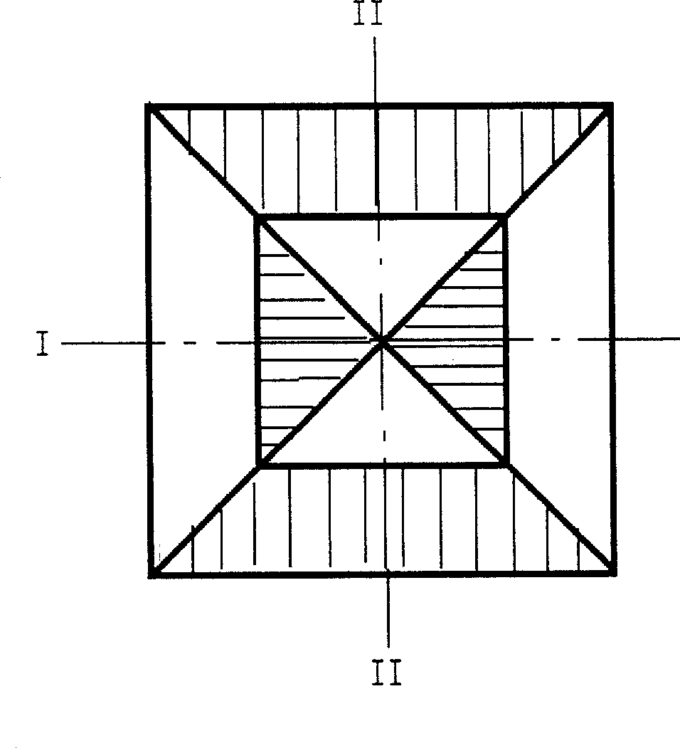
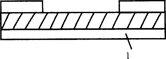
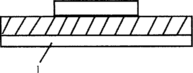
[0029] figure 1 It is a top view of a new graphic identification mark dedicated to film thickness in a semiconductor device for testing according to the first embodiment of the present invention. figure 2 yes press figure 1 A cross-sectional view of line I-I showing a new graphic identification mark dedicated to film layer thickness in the test semiconductor device according to the first embodiment of the present invention. image 3 yes press figure 1 It is a sectional view showing the II-II line of the new graphic identification mark dedicated to film layer thickness in the test semiconductor device according to the first embodiment of the present invention.

[0030] According to the first embodiment of the present invention, the special new graphic identification mark for testing the thickness of the film layer in the semiconductor device is arranged on the wafer. The outline of the new graphic identification mark is that two squares with different areas are overlapped ac...

no. 2 example

[0033] Figure 4 is a top view of a new graphic identification mark dedicated to film thickness in a semiconductor device for testing according to a second embodiment of the present invention. Figure 5 yes press Figure 4 A cross-sectional view of line I-I showing a new graphic identification mark dedicated to film layer thickness in a semiconductor device for testing according to the second embodiment of the present invention. Figure 6 yes press Figure 4 A cross-sectional view showing the II-II line of the new graphic identification mark dedicated to the film layer thickness in the test semiconductor device according to the second embodiment of the present invention.

[0034] According to the second embodiment of the present invention, the special new graphic identification mark for testing the thickness of the film layer in the semiconductor device is arranged on the wafer. The outline of the new graphic identification mark is that two rectangles with different areas are ...

no. 3 example

[0037] Figure 7 It is a top view of a new graphic identification mark dedicated to film thickness in a semiconductor device for testing according to the first embodiment of the present invention. Figure 8 yes press Figure 7 A cross-sectional view of line I-I showing a new graphic identification mark dedicated to film thickness in a semiconductor device for testing according to the third embodiment of the present invention. Figure 9 yes press Figure 7 A cross-sectional view along line II-II of a new graphic identification mark dedicated to film layer thickness in a semiconductor device for testing according to the third embodiment of the present invention.

[0038] According to the third embodiment of the present invention, the special new graphic identification mark for testing the thickness of the film layer in the semiconductor device is arranged on the wafer. The outline of the new graphic identification mark is that two hexagons with different areas are overlapped a...


PUM


Abstract

The present invention proposes one new kind of graphic recognition mark specially for testing the film thickness in semiconductor device, and the graphic recognition mark is one good comparison graph set on chip for graph recognition. The graphic recognition mark has two polygons or circles in the same geometric shape and different areas and superposed in centroid superposing mode. The polygons or circles are divided with diagonals or diameter line into several areas, of which the adjacent two are made of different materials and have different. For example, one of two adjacent areas is made of metal material, such as Al, Cu or Ag, while the other of other material, such as dielectric, oxide, nitride, etc. The two adjacent areas are constituted in different film layers and have different heights counted from the chip bottom layer.

Description

technical field [0001] The invention relates to a new pattern recognition mark, in particular to a new pattern recognition mark specially used for testing the film thickness in semiconductor devices. Background technique [0002] In advanced factories, in order to obtain semiconductor devices with consistent quality, the thickness of the film layer in the semiconductor device under manufacture is usually tested by monitoring the actual process. To do this, it is first necessary to successfully identify the pattern to test the thickness of the film layer in the semiconductor device. This requires dedicated good contrast graphics. [0003] The general method now is to arbitrarily select a device pattern on the wafer as a test mark, and as the process steps continue, the pattern selected as the test mark also changes, and it is not accurate to use such a constantly changing pattern as a pattern identification mark. To test the thickness of film layers in semiconductor devices...

Claims


Application Information

Patent Timeline
IPC IPC(8): H01L23/544
Inventor 龚新军
Owner SEMICON MFG INT (SHANGHAI) CORP
Why Eureka
Try Eureka