Substrate for ink jet head, ink jet head utilizing the same and producing method therefor
An inkjet head, substrate technology, applied in the direction of printing, etc., can solve problems such as hindering satisfactory recording or quality reliability, corrosion, etc.
- Summary
- Abstract
- Description
- Claims
- Application Information
AI Technical Summary
Problems solved by technology
Method used
Image
Examples
example 1
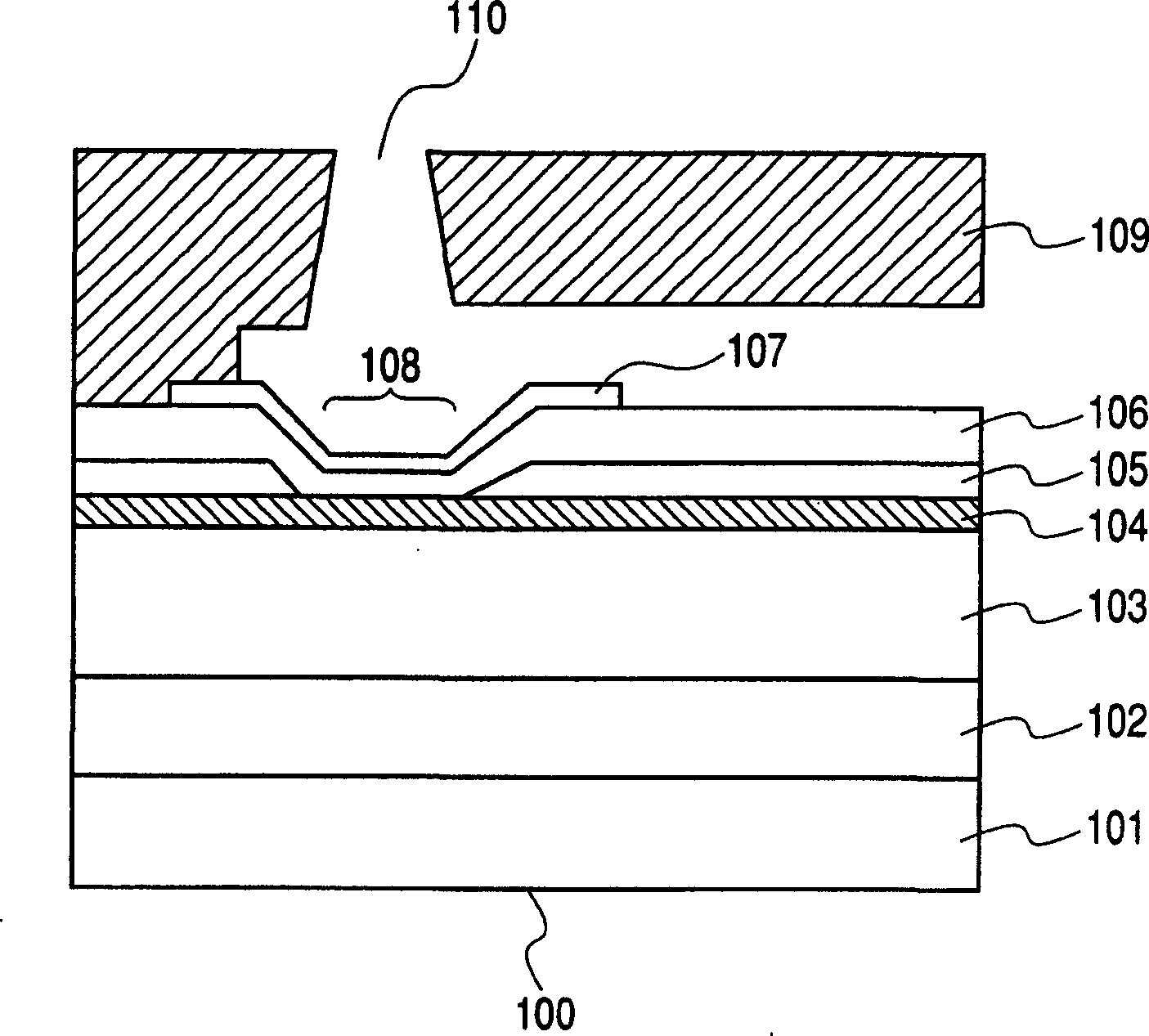
[0068] In order to simply evaluate Ta in this example 88 Cr 12 The adhesion between the film 107 (refers to the film with the composition ratio of Ta88at.% and Cr12at.%; the composition is expressed in a similar manner below) and the organic adhesion promotion film (polyetheramide resin) 307, in the pressure cooker test ( PCT) followed by a tape peel test.
[0069] The tape peel test was performed in the following manner. On the silicon wafer bearing the upper protective layer 107, an organic adhesion promoting film (polyetheramide resin) 307 having a thickness of 2 μm is formed, and a dicing knife is used to apply 10 (longitudinal) x 10 (transverse) on the organic adhesion promoting film 307 )=100 squares in a checkerboard pattern to form a 1×1mm square. After passing at 121℃ and 2.0265×10 5 PCT is performed by immersing in alkaline ink for 10 hours under the condition of Pa (2atm.). After that, the tape was applied on the squares in the checkerboard pattern and peeled off, and a...
example 8
[0083] In this example, a silicon substrate or a silicon substrate in which a driver IC is formed is used as a sample for analyzing inkjet characteristics. In the case of a silicon substrate, SiO with a thickness of 1.8 μm is formed by a thermal oxidation method, a sputtering method, or a CVD method, etc. 2 Heat accumulation layer 102 ( figure 1 ), and the silicon substrate that already has IC also undergoes the formation of SiO during the preparation process 2 The process of heat accumulation layer.
[0084] After that, SiO with a thickness of 1.2μm is formed by sputtering method or CVD method, etc. 2 Interlayer insulating film 103. After that, a 50nm thick Ta was formed by a reactive sputtering method using a Ta-Si target. 40 Si 21 N 39 Heat generating resistor 104. This operation was performed at a substrate temperature of 200°C. Then, an Al film used as the metal wiring 105 was formed to a thickness of 200 nm by a sputtering method.
[0085] Next, patterning is performed by p...
example 17
[0107] In this example, the upper protective layer 107 has a double-layer structure, and in the heat-acting portion, a double-layer structure composed of an upper Ta layer 111 and a lower TaCr layer 112 is used, and under the flow path forming element 109, only It has a single-layer structure with a lower layer 112.
[0108] More specifically, it shows the use of Ta 80 Cr 20 A case where the lower film 112 as the upper protective layer 107 and the Ta film are used as the upper film 111 are used.
[0109] By using the binary sputtering of the Ta target and the Cr target to form a Ta with Ta on the insulating layer 80 Cr 20 Composition and 130nm thickness of the lower film 112. The conditions of binary sputtering were determined by analyzing the components in advance by changing the power for Ta sputtering and for Cr sputtering. In addition, instead of binary sputtering, sputtering of a TaCr alloy target having a previously known composition can also be performed.
[0110] Then, the...
PUM
| Property | Measurement | Unit |
|---|---|---|
| Thickness | aaaaa | aaaaa |
| Thickness | aaaaa | aaaaa |
| Membrane stress | aaaaa | aaaaa |
Abstract
Description
Claims
Application Information


