Light source device, light source device producing method, and projector
A light source device and light beam technology, applied in the direction of electric light source, projection device, lighting device, etc., can solve the problems of low reflection efficiency, reduced illumination brightness of light source device, low utilization efficiency, etc., achieve easy injection management, improve utilization rate, The effect of increasing the bonding area
- Summary
- Abstract
- Description
- Claims
- Application Information
AI Technical Summary
Problems solved by technology
Method used
Image

Examples
Embodiment 1
[0105] (Structure of the projector)
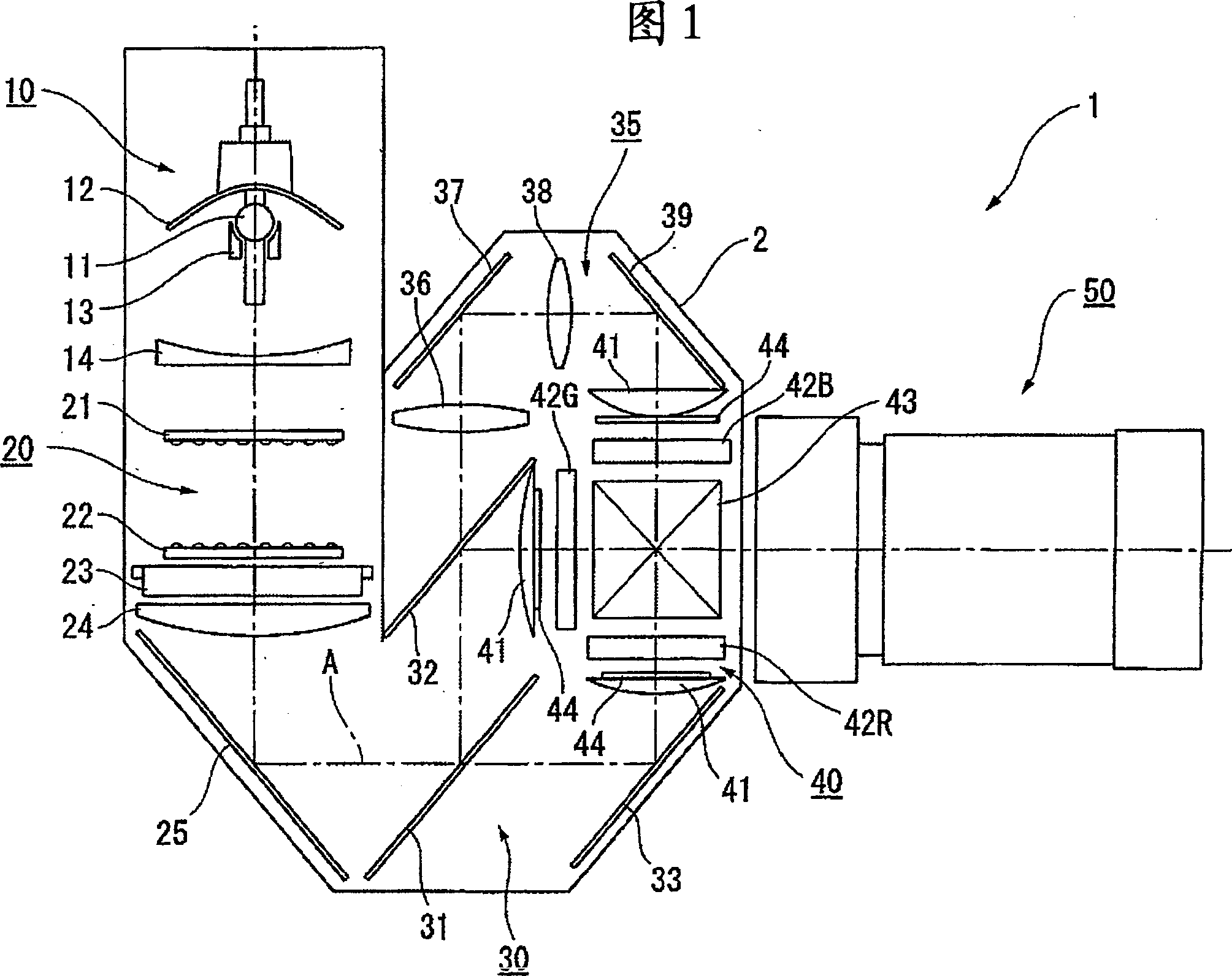
[0106] The schematic diagram shown in FIG. 1 shows the optical system of a projector 1 according to Embodiment 1 of the present invention. This projector 1 is an optical system that modulates a light beam emitted from a light source according to image information to form an optical image and enlarges and projects it on a screen. An apparatus comprising a light source device 10, a uniform illumination optical system 20, a color separation optical system 30, a relay optical system 35, an optical device 40, and a projection optical system 50, and the optical elements constituting these optical systems 20 to 35 are performed It is housed in the housing 2 for optical components in which a predetermined illumination optical axis A is set for positioning adjustment.
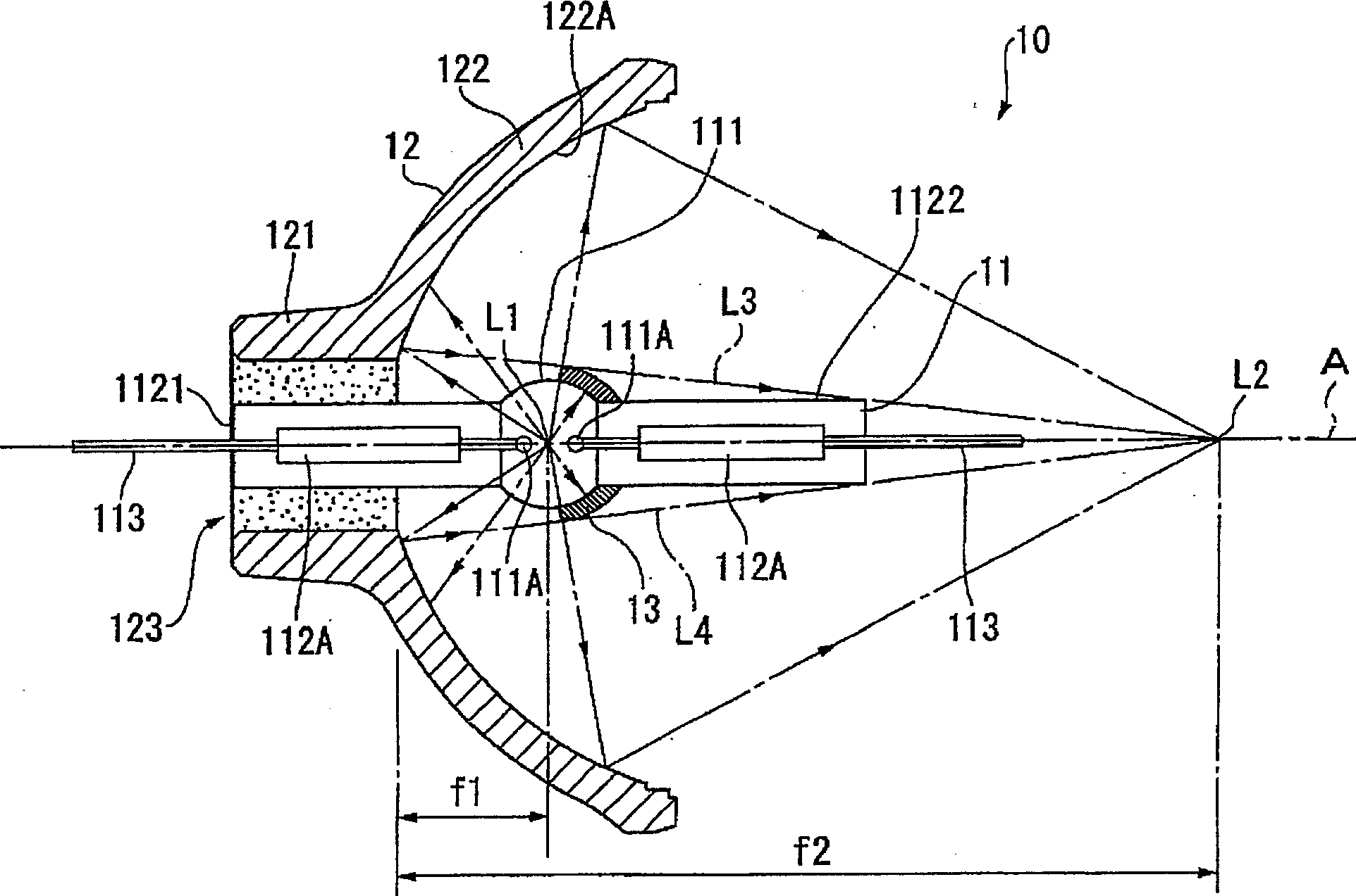
[0107] The light source device 10 is a device that adjusts the light beam emitted from the light source lamp 11 to a certain direction and emits it to illuminate the optical device ...
Embodiment 2
[0199] Next, Embodiment 2 of the present invention will be described. In addition, in the following description, the same code|symbol is attached|subjected to the part and member etc. which were already demonstrated, and the description is abbreviate|omitted or simplified.
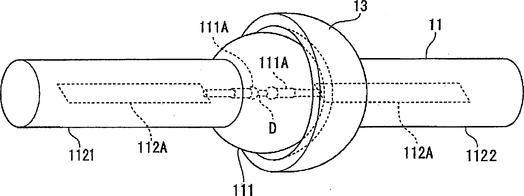
[0200] In the above-mentioned first embodiment, the outer peripheral surface 132 of the secondary reflector 13 is a curved surface shape following the curvature of the reflective surface 131, and the reflective surface 131 and the outer peripheral surface of the secondary reflector 13 are formed by grinding the cylindrical member 136. 132.
[0201] In contrast, as shown in FIGS. 14 and 15 , the sub-reflectors 71 to 74 of the second embodiment differ in that their outer peripheral surfaces 712 , 722 , 732 , and 742 are substantially cylindrical or substantially truncated cone. Such sub-mirrors 71 to 74 are formed by grinding the reflecting surface 131 of the cylindrical member 136, but the outer peripheral...
Embodiment 3
[0216] Next, Embodiment 3 of the present invention will be described. In addition, in the following description, the same code|symbol is attached|subjected to the part and member etc. which were already demonstrated, and the description is abbreviate|omitted or simplified.
[0217] The secondary reflection mirror 13 of the above-mentioned embodiment 1 or the secondary reflection mirrors 71, 73, 74 of the embodiment 2, such as Figure 4 As shown in FIG. 14 and FIG. 15 , no processing is performed on the junctions between the outer peripheral surfaces 132 , 712 , 732 , 742 and the bonding surface 134 .
[0218] In contrast, the sub-mirror 76 of the third embodiment is different in that a plurality of notched grooves 761 are formed along the ridgeline of the intersection of the outer peripheral surface 132 and the bonding surface 134 as shown in FIG. 16(A). different.
[0219] The notched grooves 761 are formed to expand outward from the periphery of the opening for inserting t...
PUM
 Abstract
Description
Claims
Application Information
 - R&D Engineer
- R&D Manager
- IP Professional
- Industry Leading Data Capabilities
- Powerful AI technology
- Patent DNA Extraction
Browse by: Latest US Patents, China's latest patents, Technical Efficacy Thesaurus, Application Domain, Technology Topic.
© 2024 PatSnap. All rights reserved.Legal|Privacy policy|Modern Slavery Act Transparency Statement|Sitemap