Electroluminescent device and method for preparing the same
An electroluminescence device, a technology of a light-emitting layer, which is applied in the direction of electroluminescence light source, electric light source, lighting device, etc.
- Summary
- Abstract
- Description
- Claims
- Application Information
AI Technical Summary
Problems solved by technology
Method used
Image
Examples
example 1
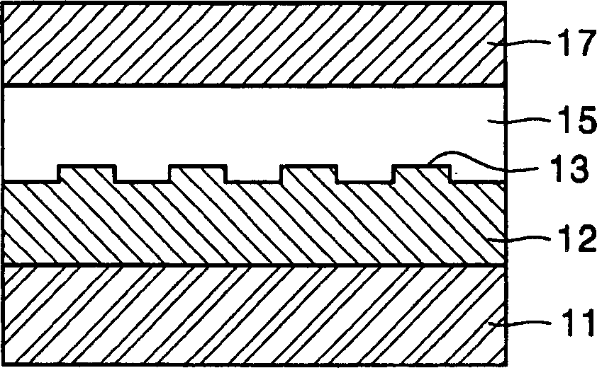
[0093] For use as the substrate and the first electrode, a glass substrate and ITO (available from Samsung Corning Co., Ltd.; sheet resistance: 15 Ω / cm 2 ; thickness: 1200 Å) was cut into a size of 50 mm × 50 mm × 0.7 mm, washed in isopropanol for 5 minutes and ultrasonically washed in pure water for 5 minutes, and subjected to UV / ozone cleaning for 30 minutes, thereby preparing ITO electrode. A 20 nm thick Au film was formed on the ITO electrode. Au films were patterned by microcontact printing (mCP) and etching, thereby forming multiple stripe-shaped Au nanopatterns on the ITO electrodes. Here, the width of each Au nanopattern is 200 nm, and the interval between two adjacent Au nanopatterns is 300 nm. Microcontact printing (mCP) and etching for forming Au nanopatterns are now described in more detail.
[0094] First, Sylgard 184A and Sylgard 184B (manufactured by Dow Corning Inc.) were mixed at a weight ratio of 10:1 in a mixing vessel to produce a PDMS forming solution. ...
example 2
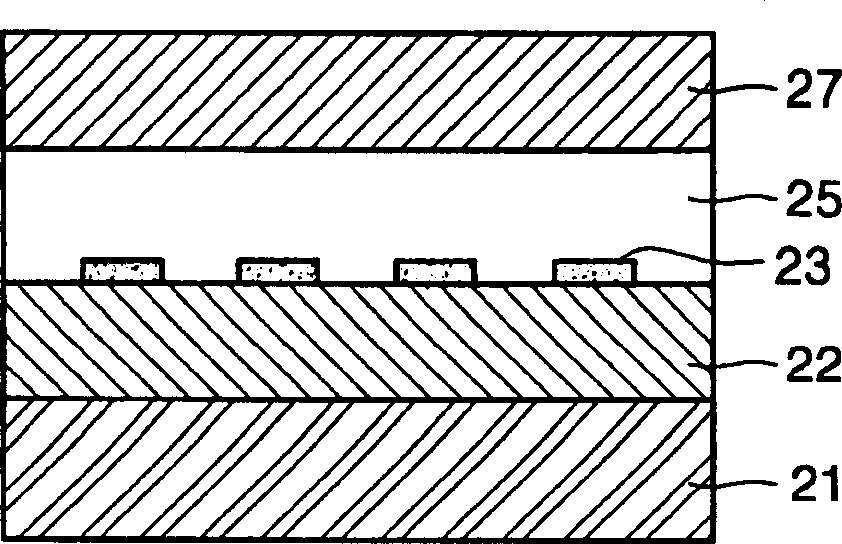
[0099] For use as the substrate and the first electrode, a glass substrate and ITO (available from Samsung Corning Co., Ltd.; sheet resistance: 15 Ω / cm 2 ; thickness: 1200 Å) was cut into a size of 50mm×50mm×0.7mm, washed in isopropanol for 5 minutes and ultrasonically cleaned in pure water for 5 minutes, and UV / ozone cleaned for 30 minutes. MEH-PPV (poly[2-methoxy-5-(2-ethylhexyloxy)-1,4-phenylene vinylene], poly[ 2-methoxy-5-(2-ethylhexyloxy)-1,4-phenylenevinylene],) made of 70nm thick light-emitting layer. The metal nanopattern-shaped second electrode (cathode) was fabricated by soft-contact lamination in the following manner.
[0100] First, Sylgard 184A and Sylgard 184B (manufactured by Dow Corning Inc.) were mixed at a weight ratio of 10:1 in a mixing vessel to produce a PDMS forming solution. The resulting PDMS forming solution is poured into the wafer forming master. The master has a bar-shaped nanopattern. A vacuum pump is used to remove pores contained in the PDM...
example 3
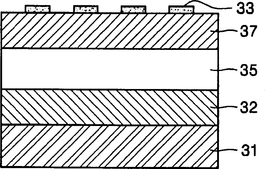
[0104] For use as the substrate and the first electrode, a glass substrate and ITO (available from Samsung Corning Co., Ltd.; sheet resistance: 15 Ω / cm 2 ; thickness: 1200 Å) was cut into a size of 50 mm×50 mm×0.7 mm, washed in isopropanol for 5 minutes and ultrasonically cleaned in pure water for 5 minutes, and UV / ozone cleaned for 30 minutes. MEH-PPV (poly[2-methoxy-5-(2-ethylhexyloxy)-1,4-phenylenevinylene], poly[2-methoxy-5-(2- Ethylhexyloxy)-1,4-phenylenevinylene]) made a 70nm thick emitting layer. A metal nanopattern-shaped second electrode (cathode) was fabricated using cold welding and soft-contact lamination in the following manner.
[0105] Firstly, Au is deposited on the entire surface of the light emitting layer. Then, Sylgard 184A and Sylgard 184B (manufactured by Dow Corning Inc.) were mixed at a weight ratio of 10:1 in a mixing vessel to produce a PDMS forming solution. Simultaneously, a master in the shape of a nanopattern (stripe) is prepared. A master of ...
PUM
| Property | Measurement | Unit |
|---|---|---|
| width | aaaaa | aaaaa |
| width | aaaaa | aaaaa |
Abstract
Description
Claims
Application Information


