Device with board abnormality detecting circuit

An anomaly detection and substrate technology, applied in the direction of measuring devices, measuring device casings, circuits, etc., can solve problems such as poor connections, reduced reliability of test devices, and inability to perform normal tests

Inactive Publication Date: 2006-08-02
ADVANTEST CORP
View PDF1 Cites 2 Cited by
  • Summary
  • Abstract
  • Description
  • Claims
  • Application Information

AI Technical Summary

Problems solved by technology

Therefore, when the DSA is attached to and detached from the motherboard, poor fitting or poor connection may occur among the multiple connectors connected between the socket board and the motherboard.
[0020] Moreover, once such a poor connection of the connector occurs, normal testing cannot be performed, the work efficiency is reduced, and the reliability of the testing device is reduced.

Method used


Image

  • Device with board abnormality detecting circuit
  • Device with board abnormality detecting circuit
  • Device with board abnormality detecting circuit

Examples


Embodiment Construction

[0048] Next, preferred embodiments of an apparatus with a substrate abnormality detection circuit according to the present invention will be described with reference to the drawings.

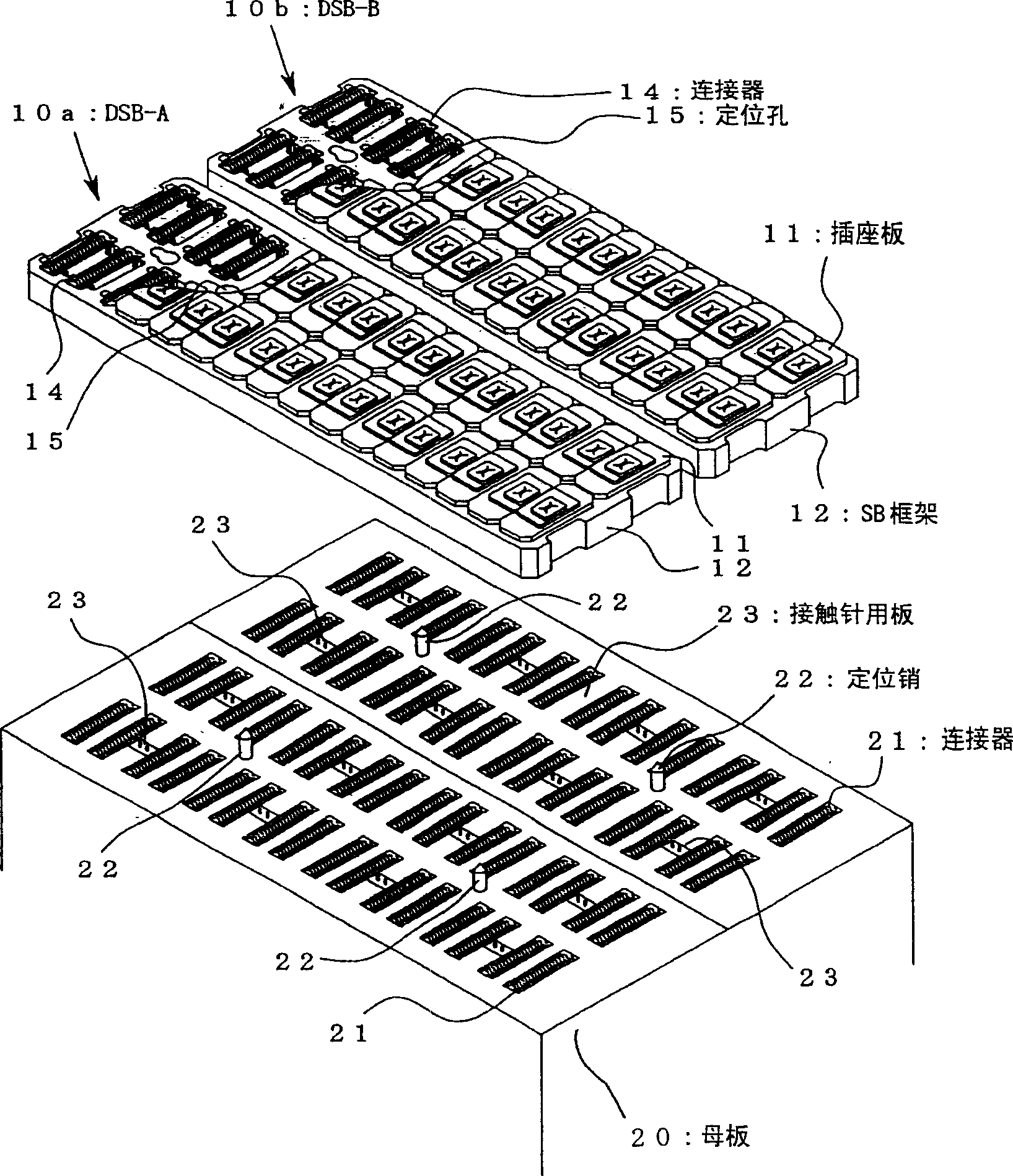
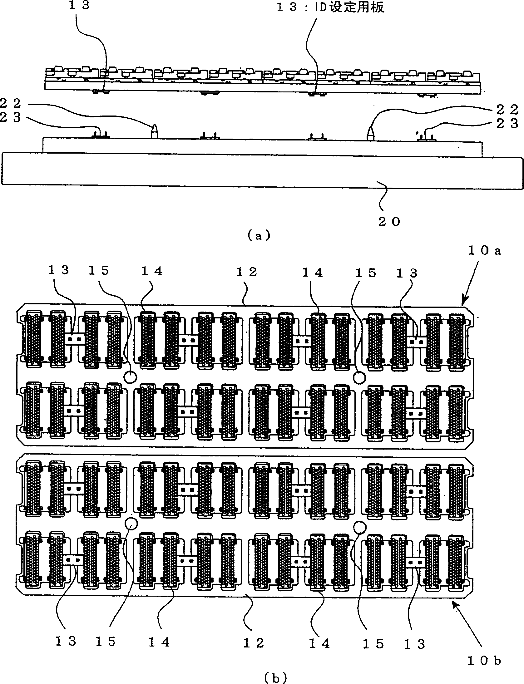
[0049] figure 1 It is an exploded perspective view showing a semiconductor testing device with a substrate abnormality detection circuit according to an embodiment of the present invention. figure 2 It shows the semiconductor testing device with the board|substrate abnormality detection circuit concerning this embodiment, (a) is a state view which removed DSA from a motherboard, (b) is the bottom view of DSA shown in (a).

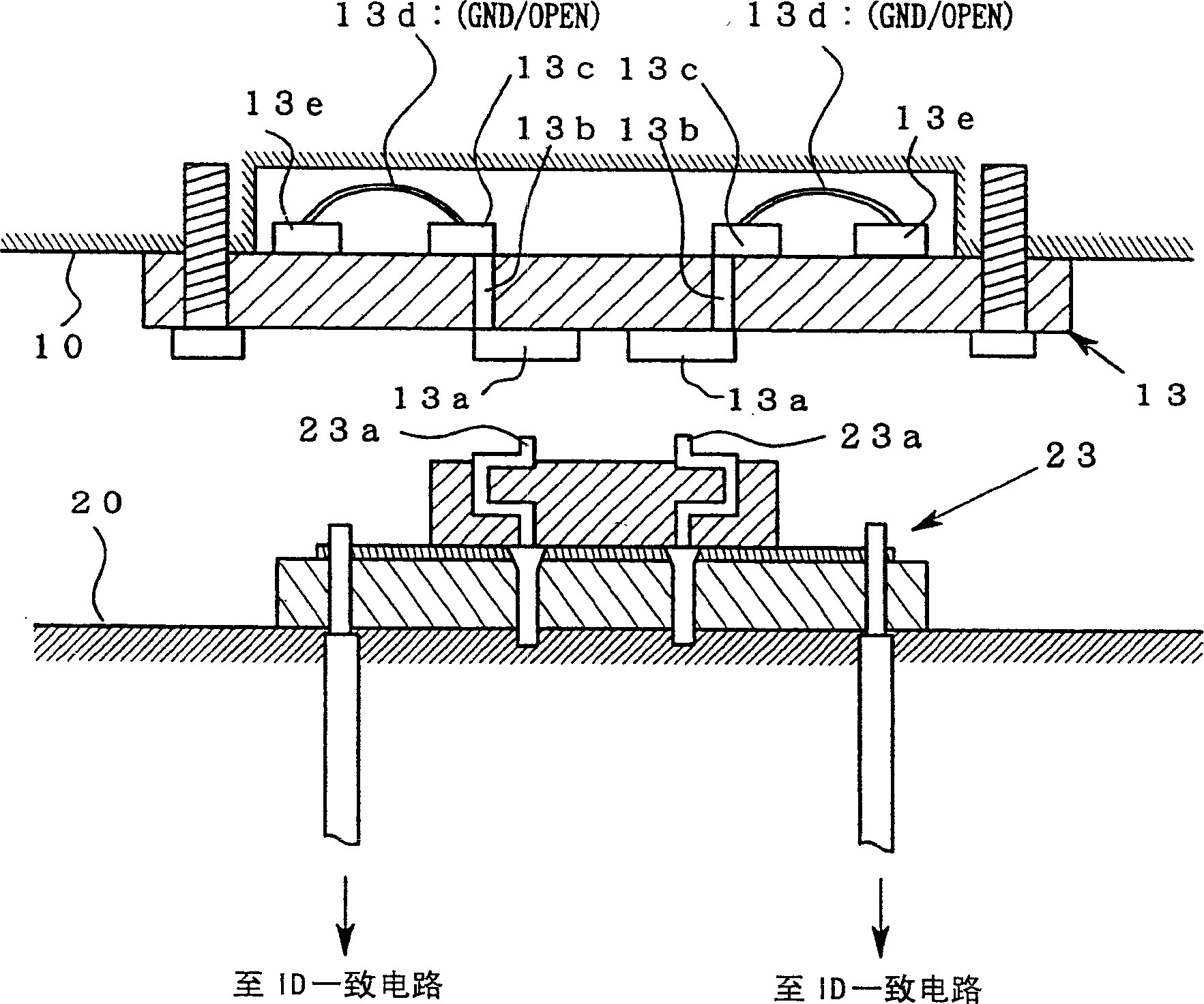
[0050] As shown in these figures, the device with a substrate abnormality detection circuit according to this embodiment is a device in which a plurality of connectors are provided on the same surface of a substrate and are connected to a plurality of connectors of a corresponding counterpart substrate. A semiconductor testing device is configured including a DSA 10 in whi...


PUM


Abstract

Misinstallation of a DSA to a semiconductor test instrument and connection failure of a connector are reliably detected and prevented. A semiconductor test instrument comprises a pair of DSAs (10a, 10b) on which socket boards are mounted and a mother board (20) having connectors to which connectors (14) of the socket boards (11) of the DSAs (10a, 10b) are connected. Each of the DSAs (10a, 10b) has an ID setting board for setting an ID number given to each DSA (10a, 10b) and outputting an ID signal representing the ID number, a coincidence circuit for receiving the outputted ID signal and detecting coincidence of the ID signal, a daisy chain circuit for receiving a signal from one of the connectors (21) of the mother board (20), transmitting the signal to all the connectors (21, 14) through the corresponding connectors (14) on the DSA side sequentially, and detecting an output signal.

Description

[0001] This application is a divisional application of application number 038049503 filed by the applicant, Advantest Co., Ltd., entitled "A device with a substrate abnormality detection circuit". technical field [0002] The present invention relates to a device that operates by connecting a substrate having one or two or more connectors to a corresponding counterpart substrate, such as a semiconductor testing device for testing semiconductor components. [0003] In particular, the present invention relates to a device having an abnormality detection circuit suitable for a semiconductor testing device used in combination with a plurality of DSAs equipped with a plurality of socket boards. Equipped with a comparator such as a coincidence circuit that detects whether the combination of the substrates is consistent or not by inputting an ID signal indicating the combination of the group of substrates, it is easy and accurate to detect the combination of different types of substra...

Claims


Application Information

Patent Timeline
Patent Type & Authority Applications(China)
IPC IPC(8): G01R31/28G01R31/26G01R1/04G01R31/02H01L21/66
CPCG01R1/0408G01R31/2808G01R31/26H01L22/00
Inventor 平野耕作
Owner ADVANTEST CORP
Why Eureka
Try Eureka