
Semiconductor designing apparatus

A semiconductor and simulation technology, applied in computer-aided design, CAD circuit design, calculation, etc., can solve the problems of wasting simulation, taking a long time, and taking a long time to detect differences, so as to prevent missed detection and shorten the time.

Inactive Publication Date: 2006-09-06
PANASONIC CORP
View PDF1 Cites 2 Cited by
  • Summary
  • Abstract
  • Description
  • Claims
  • Application Information

AI Technical Summary

Problems solved by technology

For this reason, there is a problem that it takes a long time to detect the difference
[0015] Also, there is a problem that, on the circuit diagram, the simulation mode used in each block cannot be confirmed before performing the simulation, and a simulation mode different from the intended simulation is used without confirmation
Therefore, there is a problem that it takes a long time for confirmation
[0020] Furthermore, it is not confirmed whether the simulation is performed under the same conditions between the circuits before the execution of the simulation, and when the simulation is performed under different conditions between the circuits, there is a problem of wasting the simulation.
[0021] There is also the issue of performing simulations where circuits are used incorrectly in situations that result in circuit mismatches, such as in the names, numbers, and order of pins in a block

Method used


Image

  • Semiconductor designing apparatus
  • Semiconductor designing apparatus
  • Semiconductor designing apparatus

Examples


Embodiment Construction

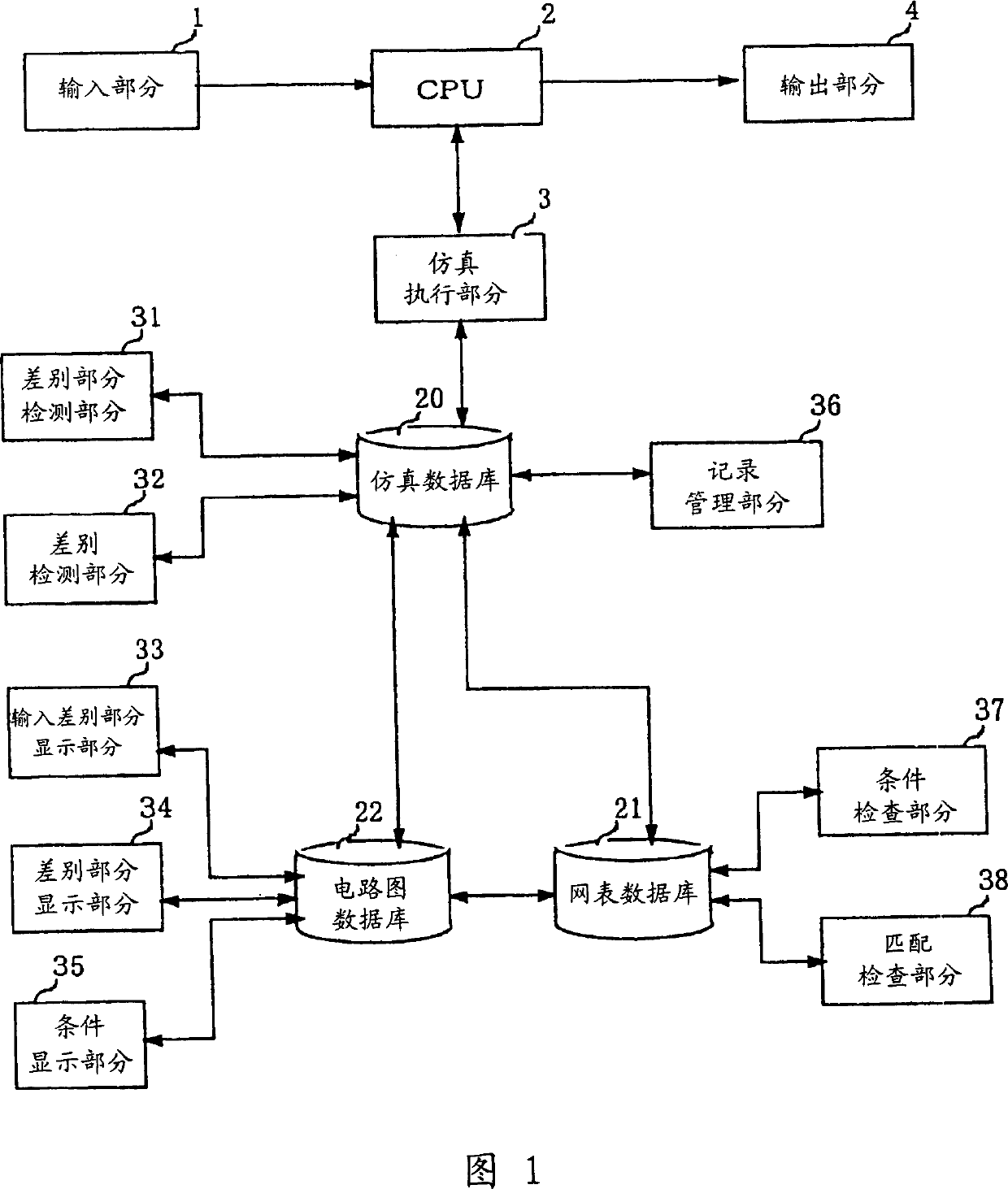
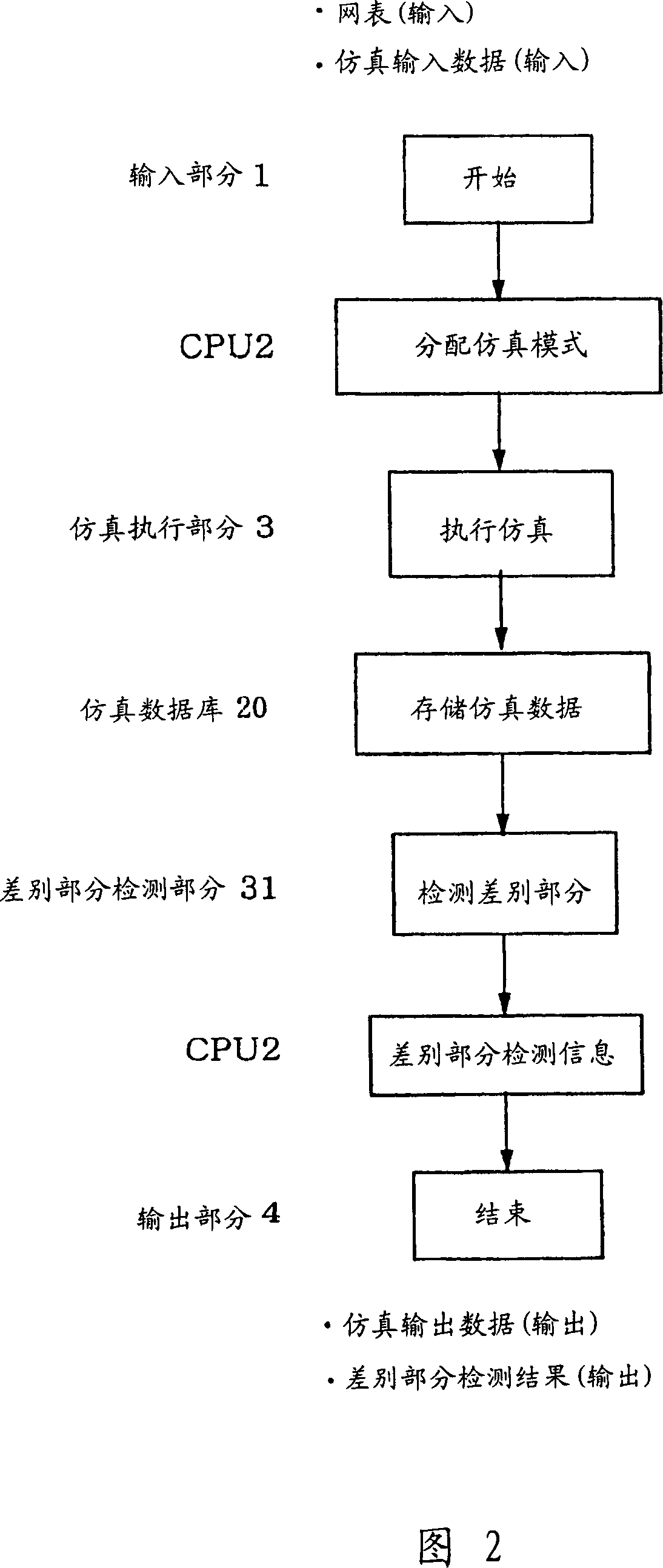
[0071] Hereinafter, embodiments of the present invention will be described with reference to these drawings. FIG. 1 is a block diagram illustrating the structure of a semiconductor design apparatus according to an embodiment of the present invention. In FIG. 1 , 1 denotes an input section, 2 denotes a CPU, 3 denotes a simulation execution section, and 4 denotes an output section, all of which have the same structure as that in FIG. 22 .

[0072] In addition, in Fig. 1, 20 represents a simulation database, 21 represents a netlist database, 22 represents a circuit diagram database, 31 represents a difference detection part, 32 represents a difference detection part, 33 represents an input difference detection part, and 34 represents a difference display part , 35 denotes a condition display section, 36 denotes a record management section, 37 denotes a condition checking section, and 38 denotes a matching checking section.

[0073] The simulation database 20 stores the processin...


PUM


Abstract

There are provided a different part detecting portion for detecting the different part of the result of a simulation, a difference detecting portion for detecting a difference in the result of a simulation, an input different part display portion for displaying any of circuits having different simulation modes which has a difference, a different part display portion for displaying a circuit having a difference in the result of a simulation, a condition display portion for displaying, on a circuit diagram, an option to be used in a simulation, a record managing portion for managing the execution history of the result of a simulation, a condition checking portion for ascertaining whether or not a condition is accurately set in each circuit in the execution of a simulation, and a match checking portion for confirming the non-coincidence of the names and numbers of pins between the simulation modes.

Description

technical field [0001] The present invention relates to a semiconductor design device for designing a semiconductor circuit. Background technique [0002] Heretofore, in the case of designing a semiconductor memory circuit or an analog circuit, functions are digitally verified by using C language at an early stage of the design stage, and analog circuit simulation is performed for each block by using SPICE as the design stage progresses. Thus, the design can be checked. [0003] Moreover, in recent years, analog / digital hybrid simulators have reached the level of practical application, and analog and digital simulations can be performed mixedly (for example, see "Analog / Digital Hybrid Simulator", Nikkei Electronics (10-14) Supplement, Nikkei BP LLC, October 14, 1996, p. 120). [0004] Accordingly, the simulation mode to be used for each block corresponding to the progress of the design stage can be selectively converted to digital or analog, and simulation can be performed...

Claims


Application Information

Patent Timeline
Patent Type & Authority Applications(China)
IPC IPC(8): G06F17/50
CPCG06F17/5036G06F17/5022G06F30/33G06F30/367
Inventor 石山裕浩
Owner PANASONIC CORP
Learn More