Method for manufacturing semiconductor element

A technology of semiconductors and components, applied in the field of source/drain regions of complementary metal oxide semiconductor transistors, which can solve the problems of reducing the drive current of PMOS components, easily increasing source/drain resistance, and depleting gate depletion

Active Publication Date: 2007-02-14
TAIWAN SEMICON MFG CO LTD
View PDF0 Cites 7 Cited by
  • Summary
  • Abstract
  • Description
  • Claims
  • Application Information

AI Technical Summary

Problems solved by technology

However, the aforementioned shrinking source / drain region size tends to increase source / drain resistance and worsen its polysilicon gate depletion.
Therefore, shrinking the source / drain junction will reduce the drive current of the PMOS device.

Method used


Image

  • Method for manufacturing semiconductor element
  • Method for manufacturing semiconductor element
  • Method for manufacturing semiconductor element

Examples


Embodiment Construction

[0042] The methods for making and using the current commonly used embodiments of the present invention will be described in detail below. The present invention presents many implementable innovative concepts that can be implemented in a wide variety of specific situations. The specific embodiments discussed herein are intended merely to illustrate specific ways to make and practice the invention, and do not limit the invention to the specific scope.

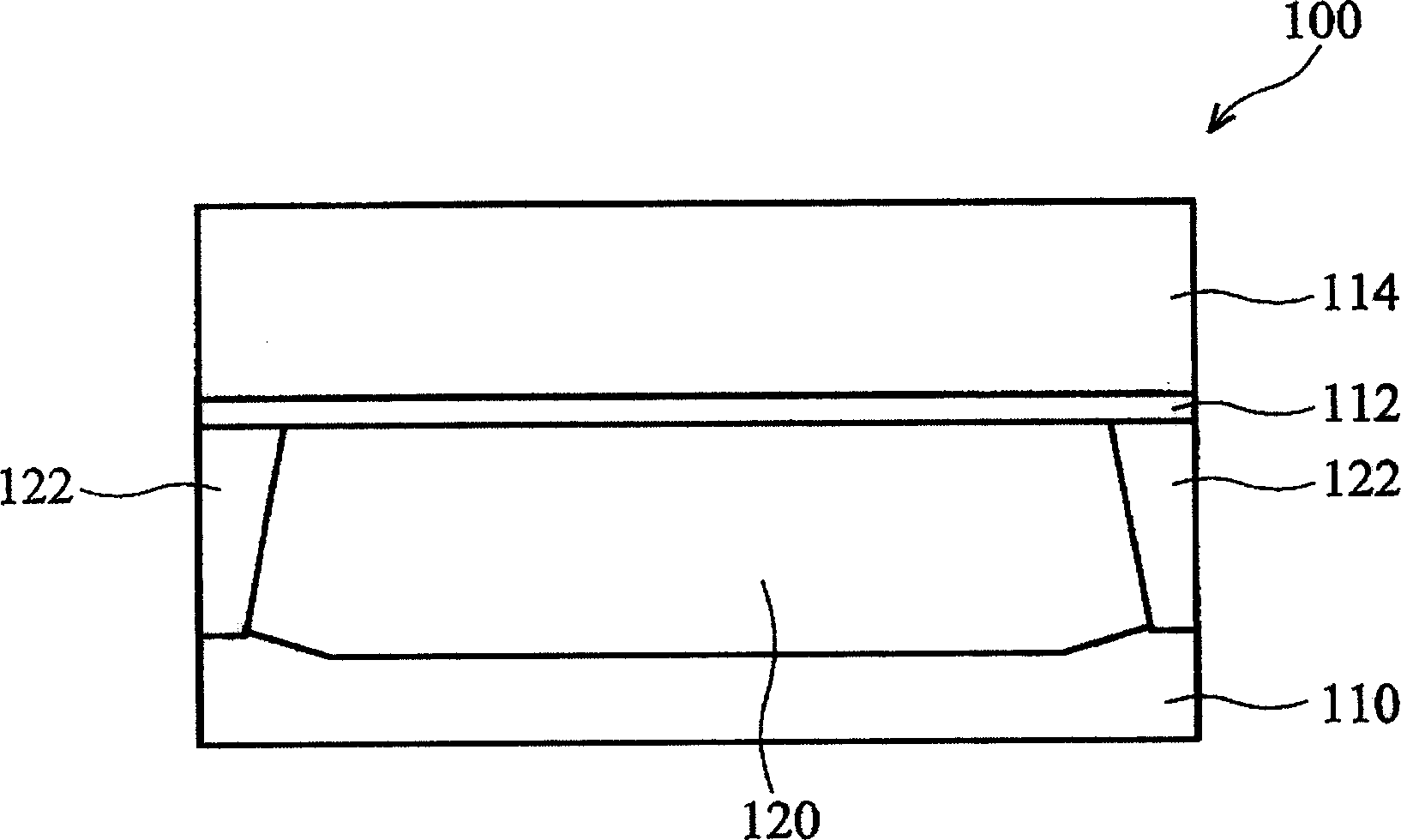
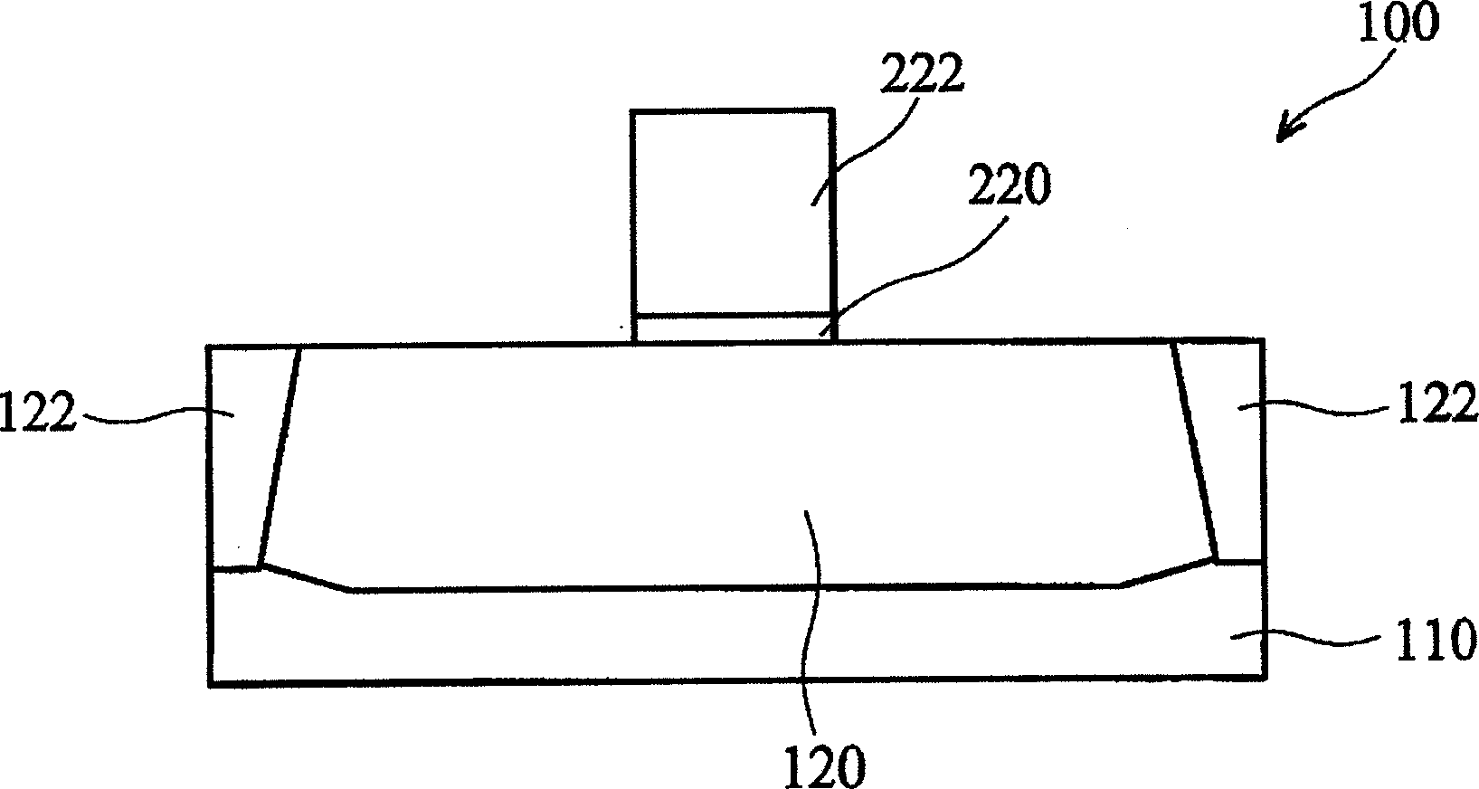
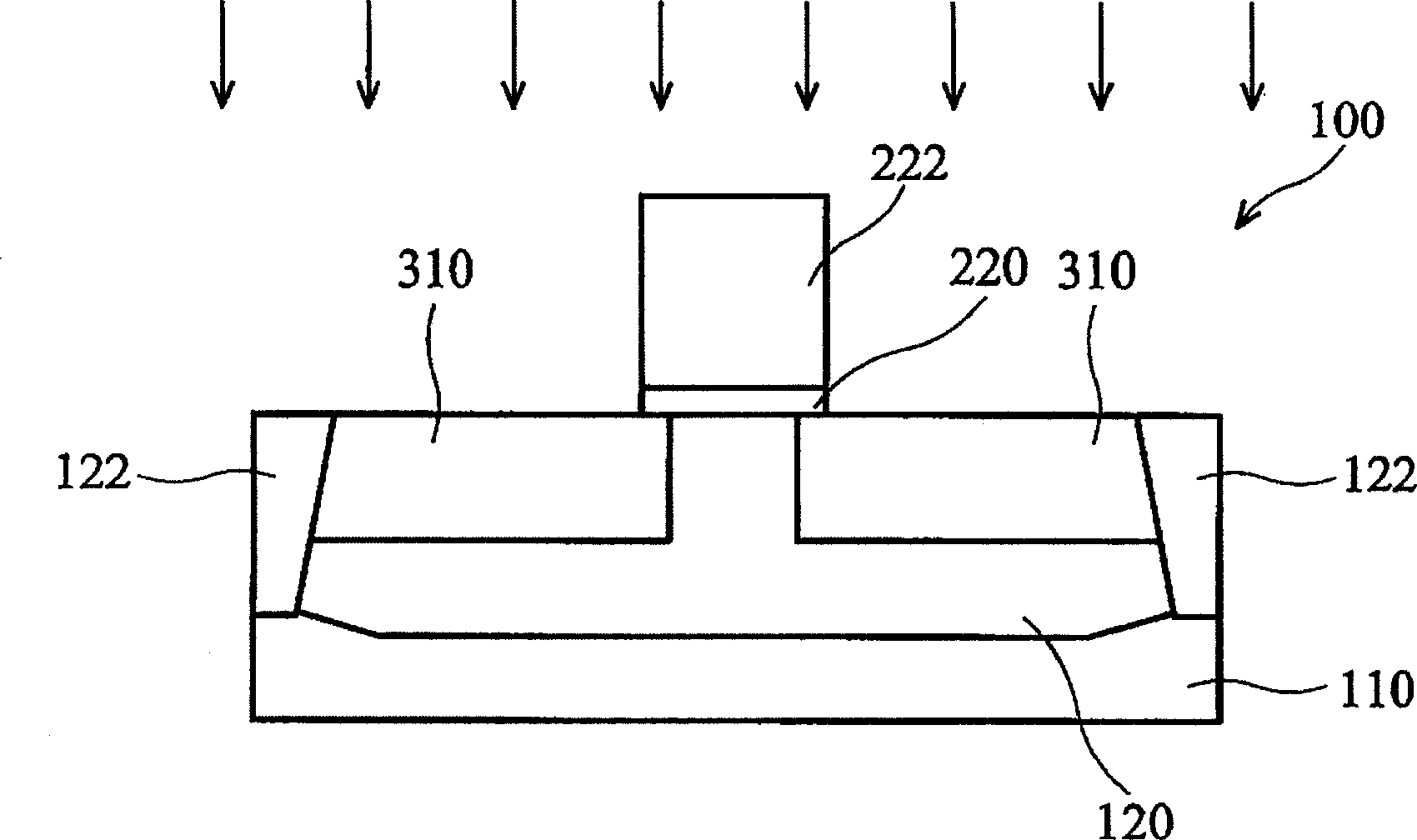
[0043] Figure 1 to Figure 6 An embodiment is described, wherein an amorphization process and a co-implant process are used to fabricate p-type metal oxide semiconductor (PMOS) transistors according to an embodiment of the present invention. Amorphization and simultaneous implantation processes have been found to limit lateral / vertical diffusion of source / drain implants. Therefore, higher dopant concentrations can be used to create shallower source / drain regions while reducing or eliminating short channel effects. For the conv...


PUM


Abstract

The invention proposes a method for manufacturing a semiconductor element which has shallow, high-dopant concentration source / drain regions. The manufacturing method is provided that, a gate electrode is formed on a substrate, and the source / drain regions of the substrate are transformed into an amorphous state by implanting ions. A co-implantation process is performed to implant ions in the source / drain regions. Thereafter, one or more implants may be performed to form the LDD and source / drain regions and the substrate is recrystallized. The amorphous regions and the co-implantation regions effectively confine or reduce the diffusion of the ions used to form the LDD and source / drain regions.

Description

technical field [0001] The present invention relates to semiconductor devices, and more particularly to source / drain regions of complementary metal oxide semiconductor (CMOS) transistors. Background technique [0002] CMOS technology is the mainstream semiconductor technology for manufacturing Ultra Large Scale Integration (ULSI) today. Over the past few decades, the scaling of semiconductor structures has dramatically increased the speed, performance, circuit density, and cost per computing unit of semiconductor chips. However, as the size of CMOS components continues to decrease, semiconductor technology faces greater challenges. [0003] As an example, when the length of the gate electrode of a CMOS transistor becomes smaller, especially when the gate length is less than 30 nm, the interaction between the source and drain regions and the channel increases, and the source and drain regions interact with the channel. potential to increase with the influence of the gate di...

Claims


Application Information

Patent Timeline
Patent Type & Authority Applications(China)
IPC IPC(8): H01L21/336H01L21/8238
CPCH01L29/7833H01L29/66772H01L21/26506H01L21/26513H01L29/6659H01L21/2658
Inventor 陈建豪聂俊峰李资良
Owner TAIWAN SEMICON MFG CO LTD
Why Eureka
Try Eureka