

Semiconductor device
一种半导体、器件的技术,应用在有效抑制软误差的半导体器件布局领域,能够解决无法电路应用等问题,达到最小化总布局面积、防止反转、增加节点电容的效果
- Summary
- Abstract
- Description
- Claims
- Application Information
AI Technical Summary
Problems solved by technology
Method used
Image

Examples
no. 1 example
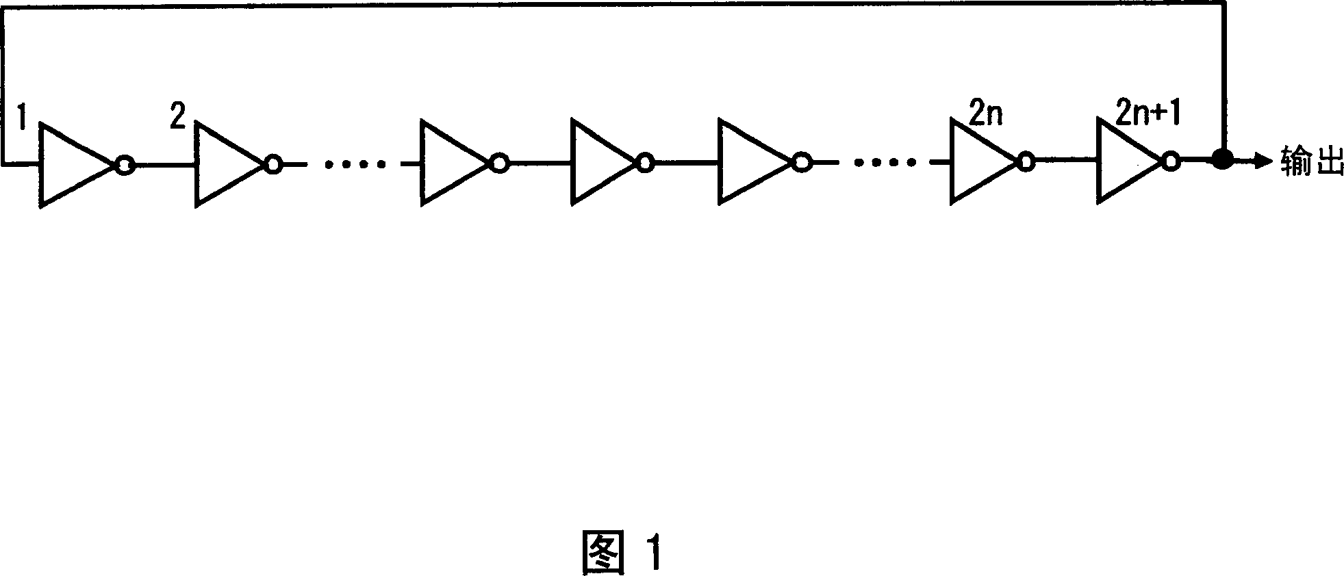
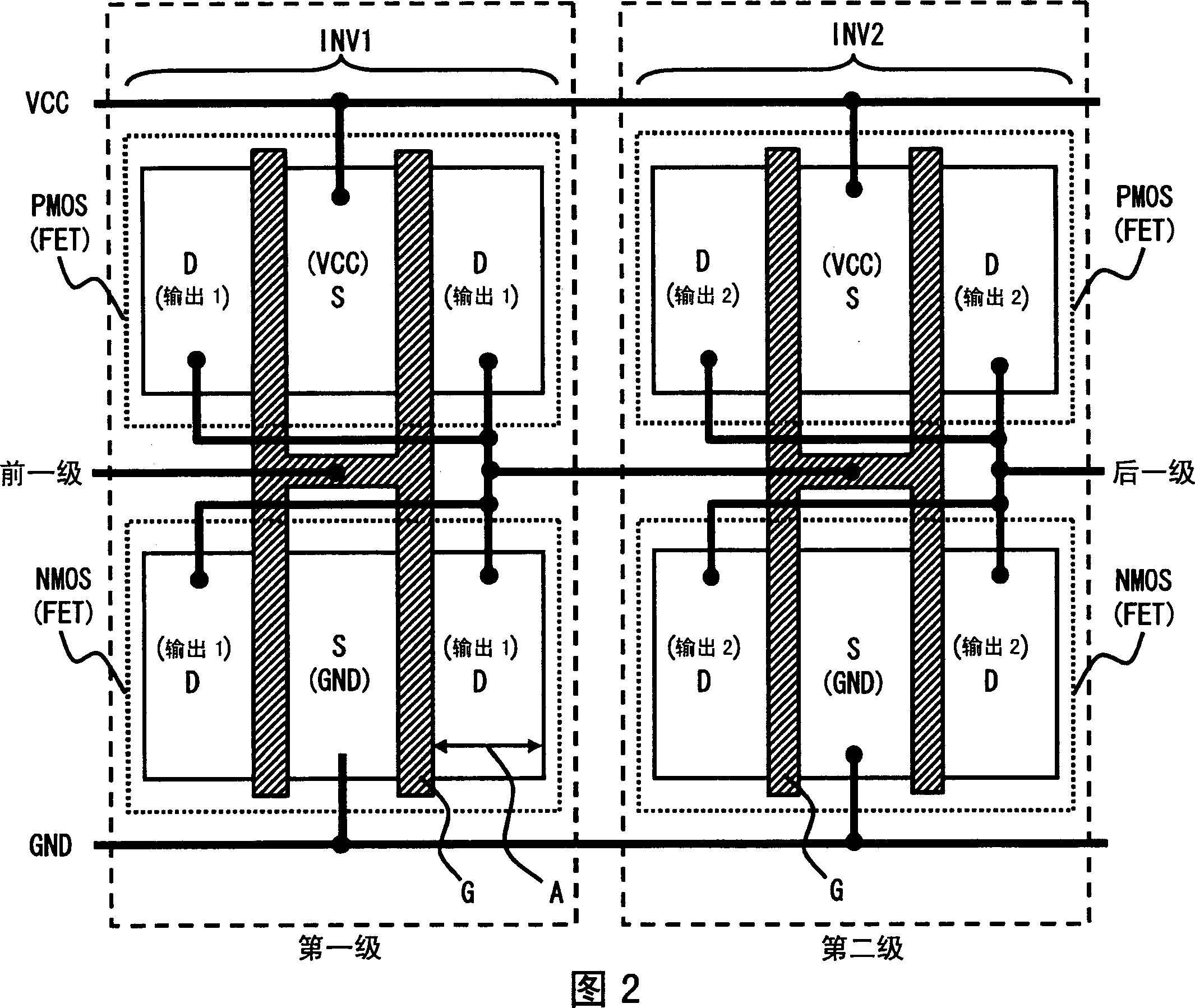
[0040] FIG. 1 shows an oscillator circuit (for example, a ring oscillator circuit) according to a first embodiment of the present invention. As shown in FIG. 1, the ring oscillator circuit includes an odd number of logic circuits (eg, inverter circuits) connected in series. For example, the ring oscillator circuit of this embodiment is formed on a silicon semiconductor substrate. FIG. 2 shows the layout of two of the inverter circuits making up the ring oscillator circuit.
[0041]Referring to FIG. 2, the layout of the first embodiment will be described in detail. As shown in FIG. 2, each inverter circuit has two field effect transistors (eg, a PMOS transistor and an NMOS transistor). The inverter circuits are connected in series to operate as a ring oscillator circuit. In the following description, a direction from left to right in FIG. 2 is referred to as an X direction, and an upward direction in FIG. 2 is referred to as a Y direction. The description focuses on an inve...
no. 2 example
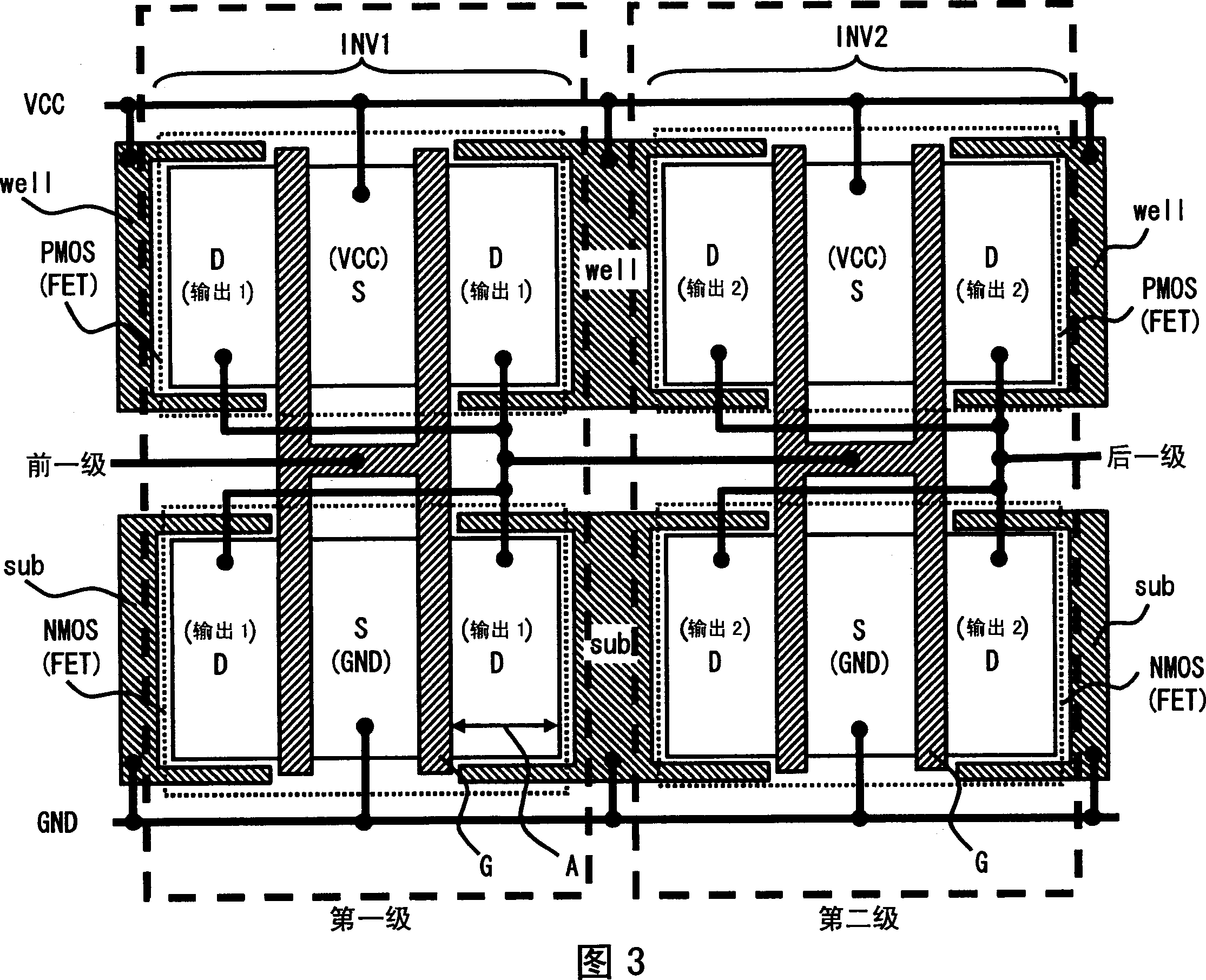
[0054] Fig. 3 shows the layout of an inverter circuit according to a second embodiment of the present invention. The layout of the inverter circuit of the second embodiment differs from that of the inverter circuit of the first embodiment in that a well potential diffusion layer region well (N-type diffusion layer) is added between the two inverter circuits. layer) and the substrate potential diffusion layer region sub (P-type diffusion layer). The same reference numerals are assigned to the same layout parts as those of the first embodiment, and descriptions thereof are omitted here.
[0055] The layout of the inverter circuit of the second embodiment is as follows. The inverter circuit of the second embodiment has a well potential diffusion layer region well and a substrate potential diffusion layer region sub provided between two adjacent inverter circuits. The well potential diffusion layer region well is connected to the power supply voltage VCC, and is formed between t...
no. 3 example
[0059] FIG. 4 shows the layout of an inverter circuit according to a third embodiment of the present invention. The layout of the inverter circuit of the third embodiment is different from that of the second embodiment in that the number of source regions and drain regions of each transistor is increased. The same reference numerals are assigned to the same layout parts as those of the first embodiment, and descriptions thereof are omitted here.
[0060] The layout of the inverter circuit of the third embodiment is described in detail below. The layout of the inverter circuit of the third embodiment is substantially the same as that of the inverter circuit of the first embodiment. The following description focuses on differences between the first embodiment and the third embodiment.
[0061] The gate G of this embodiment extends in the Y direction and has a rectangular shape. Each transistor pair (NMOS transistor and PMOS transistor) has 4 gates G, and these 4 gates G are c...
PUM
 Abstract
Description
Claims
Application Information