Display panel and method for manufacturing same

A manufacturing method and technology for display panels, applied in optics, lenses, instruments, etc., can solve problems such as difficulty in achieving shape uniformity of 2-layer microlenses

Inactive Publication Date: 2007-03-28
SHARP KK
View PDF6 Cites 15 Cited by
  • Summary
  • Abstract
  • Description
  • Claims
  • Application Information

AI Technical Summary

Problems solved by technology

Therefore, it is difficult to achieve shape uniformity of 2-layer microlenses

Method used


Image

  • Display panel and method for manufacturing same
  • Display panel and method for manufacturing same
  • Display panel and method for manufacturing same

Examples


Embodiment Construction

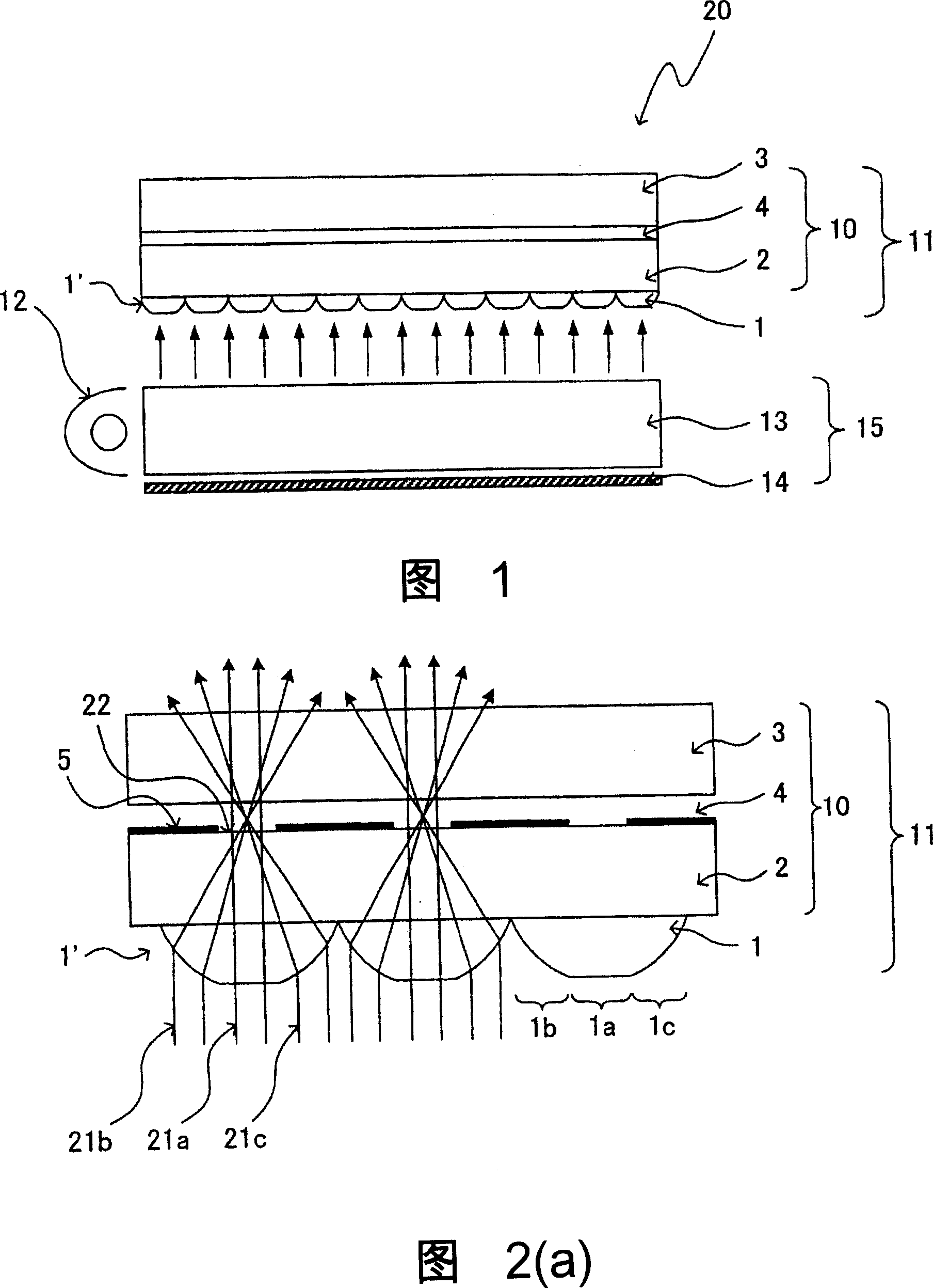
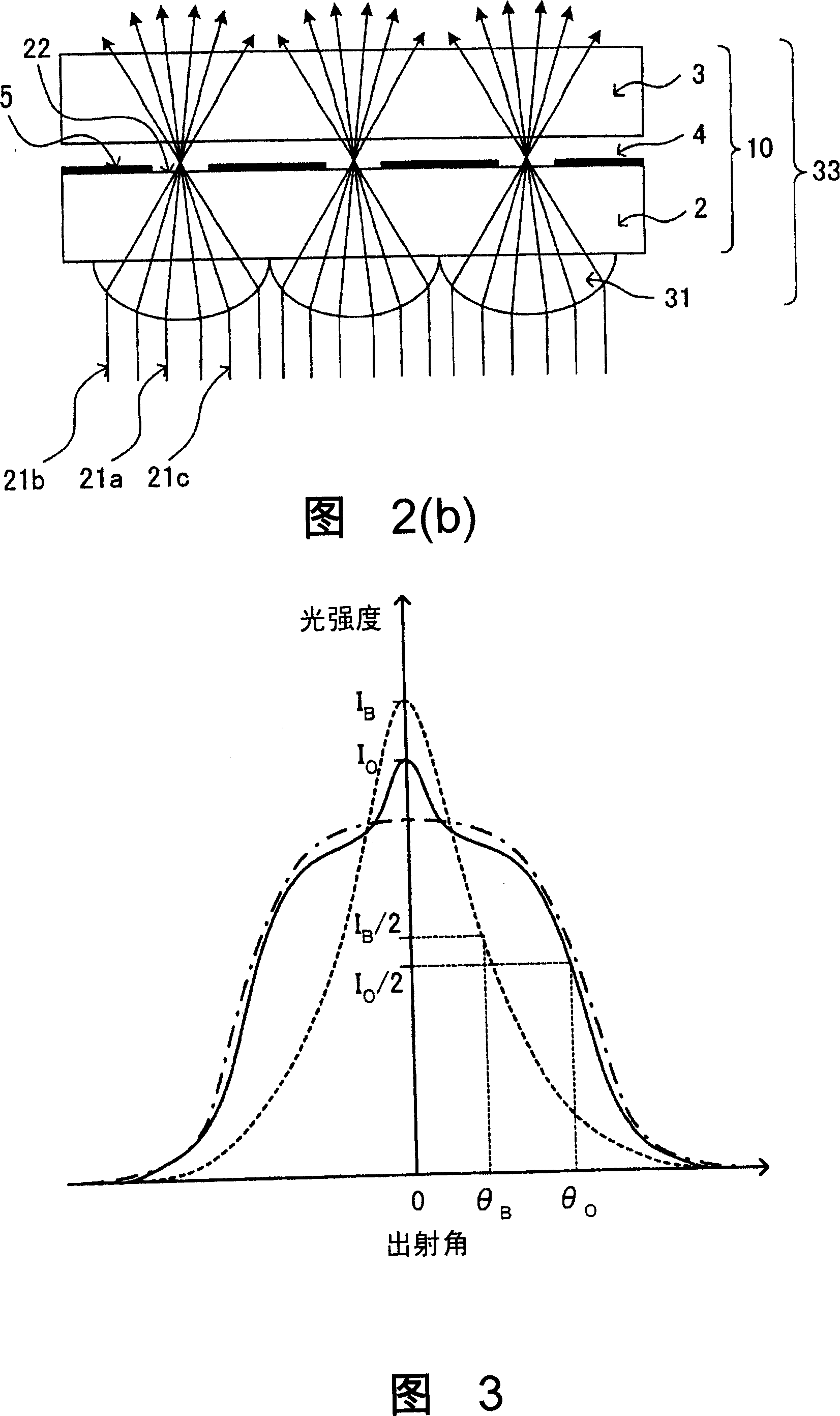
[0049] An embodiment of the present invention is described with the drawings. FIG. 1 is a cross-sectional view diagrammatically showing the composition of a liquid crystal display panel (display panel) 11 and a liquid crystal display device 20 including the display panel according to the present embodiment. The liquid crystal display device 20 is a semi-transmissive liquid crystal display device, which uses the backlight light penetrating the liquid crystal display panel 11 to display under dark lighting, and reflects the light incident on the display surface of the liquid crystal display panel 11 from the surroundings under bright lighting. to display. Therefore, the liquid crystal display device 20 is a non-self-luminous display device.

[0050] As shown in FIG. 1 , the liquid crystal display device 20 has a liquid crystal display panel 11 and a backlight 15 with high directivity.

[0051] The components of the liquid crystal display panel 11 include: a TFT substrate 2 pro...


PUM

PropertyMeasurementUnit
refractive indexaaaaaaaaaa

Abstract

A microlens array 1' constituted of a plurality of microlenses 1 each having a flat section 1a at a top portion is arranged on one side of a liquid crystal display panel 11 from which side light from a backlight enters. Each microlens 1 is so formed that its width is equal to the pixel pitch. Consequently, the viewing angle can be widened without deteriorating front luminance.

Description

technical field [0001] The present invention relates to a non-self-luminous display panel and its manufacturing method, in particular to a display panel with a microlens array for improving light utilization efficiency and its manufacturing method. Background technique [0002] In recent years, liquid crystal display devices, which are non-self-luminous display devices, have been widely used as display devices used in monitors, projectors, portable information terminals, mobile phones, and the like. The non-self-luminous display device represented by the liquid crystal display device generally changes the transmittance (or reflectance) of the display panel by a driving signal, and modulates the light intensity from the light source irradiating the display panel to display images and characters. Such display devices include a direct-view display device for directly viewing images displayed on a display panel, and a projection display device (projector) for projecting images d...

Claims


Application Information

Patent Timeline
Patent Type & Authority Applications(China)
IPC IPC(8): G02F1/1335G02F1/13357G02B3/00G09F9/00
CPCG02F1/133526G02B3/0031G02F1/133555G02F1/133512G02B3/005
Inventor 冈田训明中西浩
Owner SHARP KK
Why Eureka
Try Eureka