Surface structure of flip-chip substrate
A surface structure, flip-chip technology, applied in electrical components, electrical solid devices, circuits, etc., can solve the problems of difficult control of pre-solder printing process quality, solder ball falling, and uneven pre-solder amount.
- Summary
- Abstract
- Description
- Claims
- Application Information
AI Technical Summary
Problems solved by technology
Method used
Image

Examples
Embodiment Construction
[0033] In order to further understand the features and technical content of the present invention, please refer to the following detailed description and accompanying drawings of the present invention. However, the drawings are only for reference and auxiliary description, and are not intended to limit the present invention.
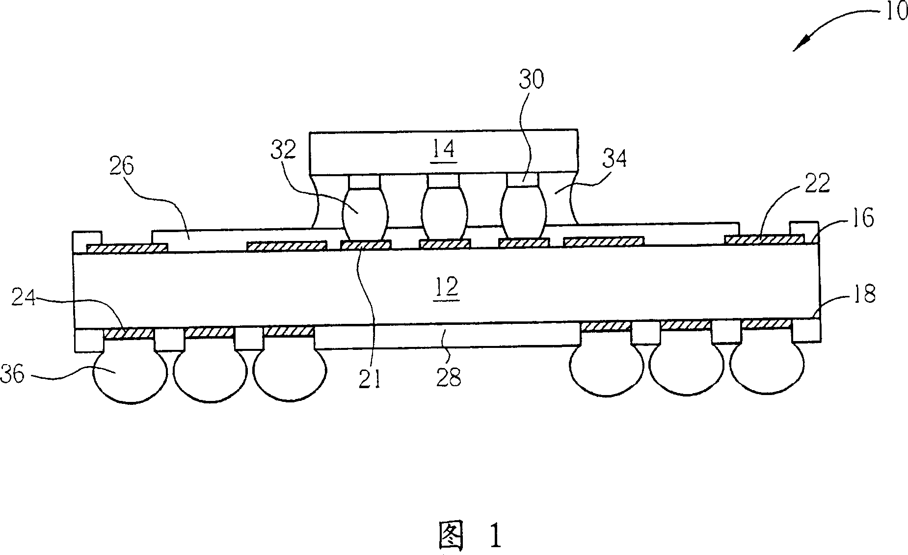
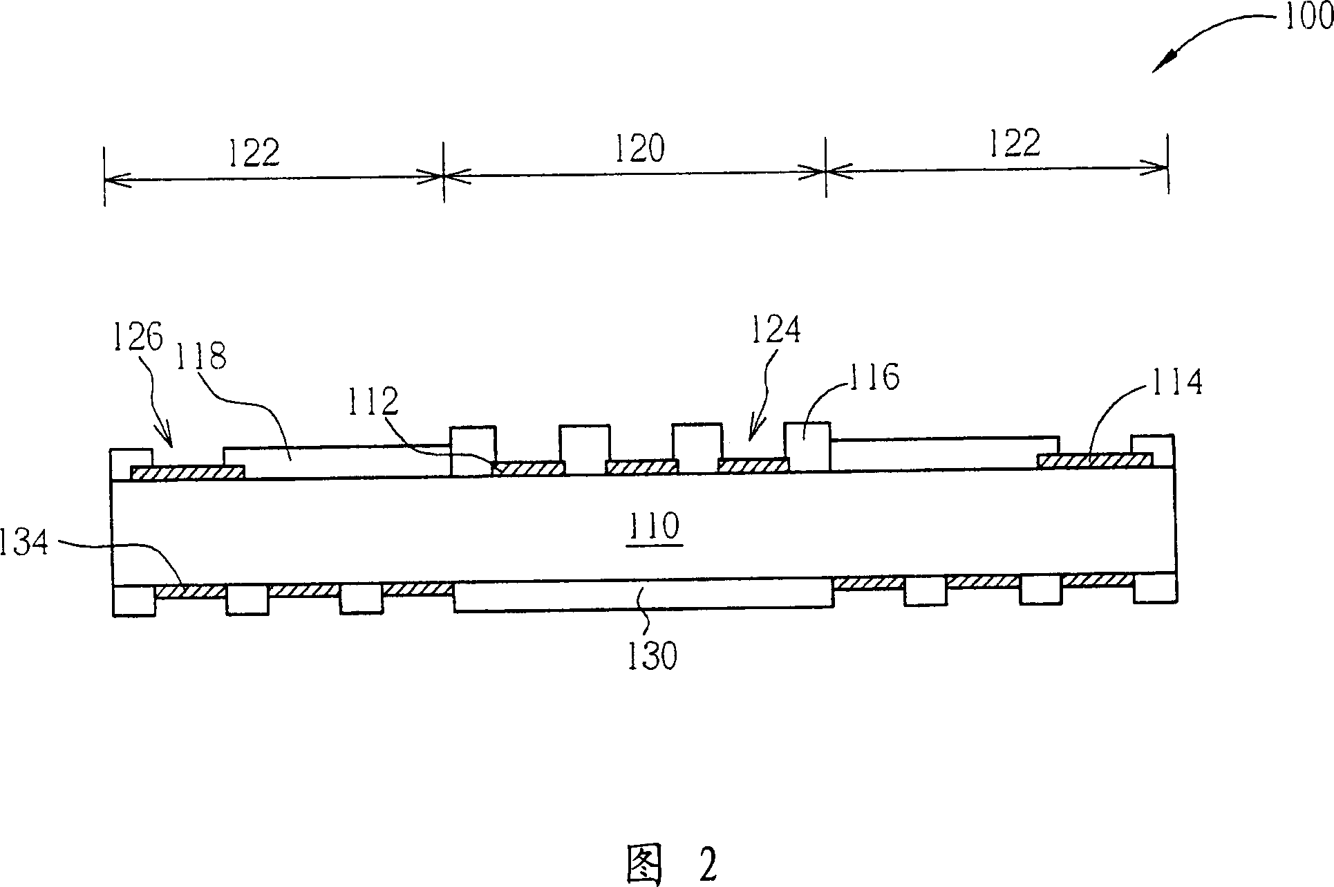
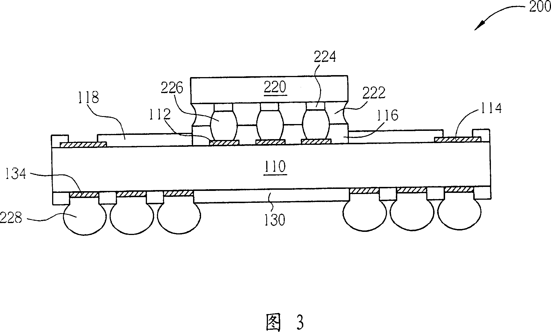
[0034] Please refer to FIG. 2 to FIG. 4 , which are schematic diagrams of the flip chip substrate 100 of the present invention. As shown in FIG. 2 , the flip-chip substrate 100 of the present invention includes a substrate 110 , and the substrate 110 defines a chip connection area 120 and a passive component connection area 122 . In the present invention, a known connection pad process is used to simultaneously manufacture a plurality of first electrical connection pads 112 and second electrical connection pads 114 in the chip connection area 120 and the passive element connection area 122 on the surface of the substrate 110, They are respectively used ...
PUM
 Abstract
Description
Claims
Application Information
 - R&D
- Intellectual Property
- Life Sciences
- Materials
- Tech Scout
- Unparalleled Data Quality
- Higher Quality Content
- 60% Fewer Hallucinations
Browse by: Latest US Patents, China's latest patents, Technical Efficacy Thesaurus, Application Domain, Technology Topic, Popular Technical Reports.
© 2025 PatSnap. All rights reserved.Legal|Privacy policy|Modern Slavery Act Transparency Statement|Sitemap|About US| Contact US: help@patsnap.com