This helps you quickly interpret patents by identifying the three key elements:
Problems solved by technology
Method used
Benefits of technology
Problems solved by technology
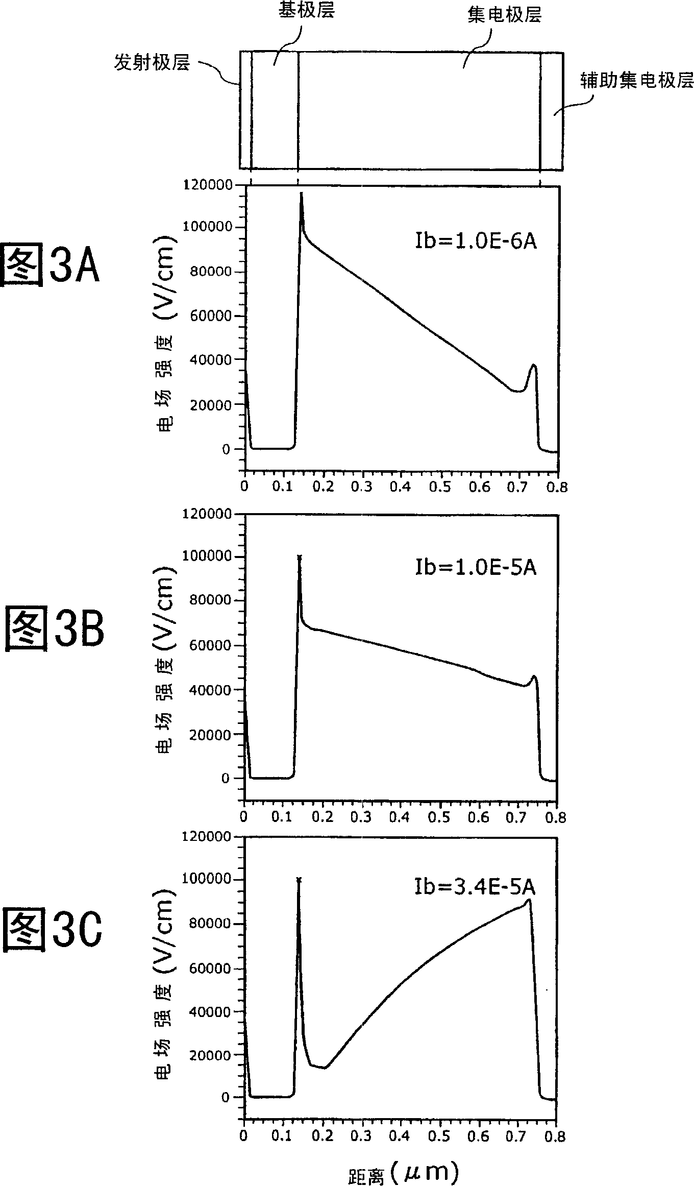
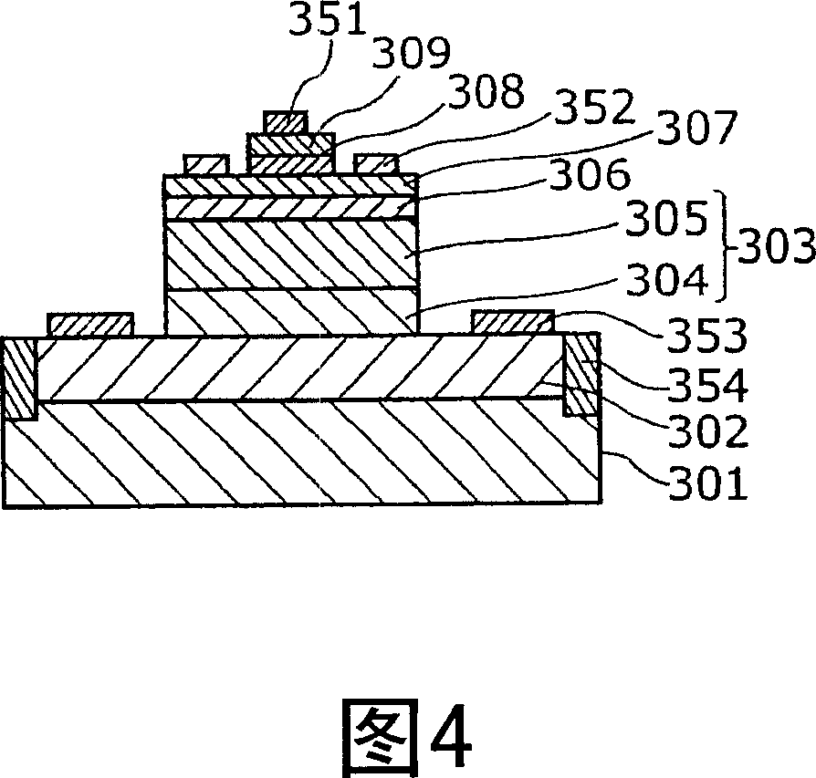
As a result, the collector resistance increases due to the conduction band discontinuity, or the high-frequency characteristics of the transistor deteriorate due to carrier accumulation and retention effects.
In addition, when ordered InGaP is used for the etch stop layer, localized electric field concentration occurs due to carrier location in InGaP, which deteriorates breakdown resistance.
Further, it is also considered that when a material different from that described above is used as an etching stopper layer, the crystallinity deteriorates, the defect level of the base layer or the base-emitter interface increases, causing β decay or lowering of reliability
Method used
Image
Click on the blue label to locate the original text in one second.
Reading with bidirectional positioning of images and text.
Examples
no. 1 Embodiment approach
[0075] Fig. 6 is a cross-sectional view showing the structure of the HBT in the first embodiment of the present invention.
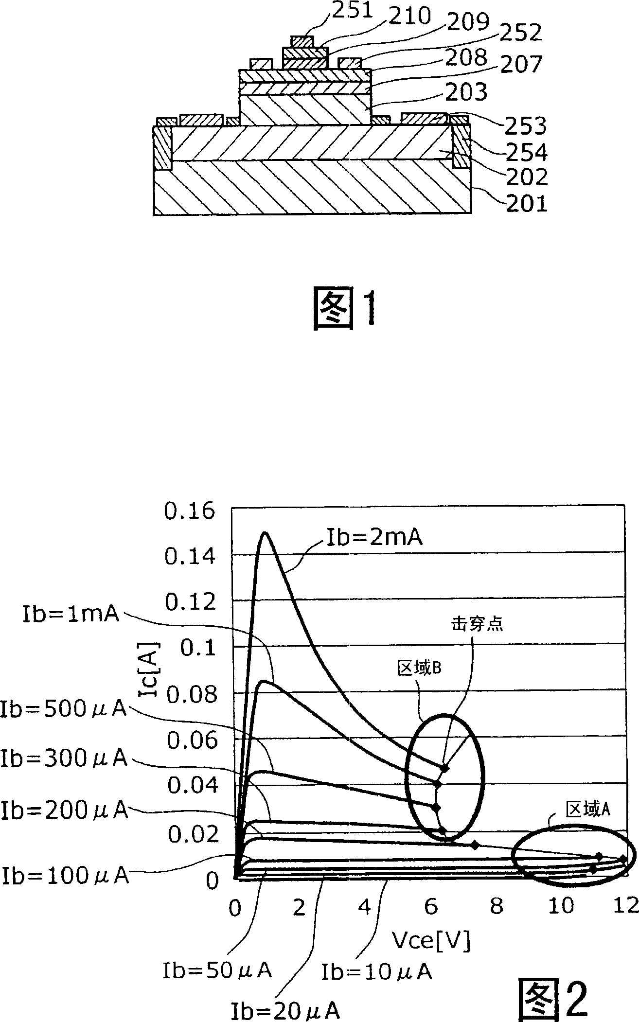
[0076] As shown in FIG. 6, in this HBT, on a substrate 101 made of semi-insulating GaAs, a 5×10 18 cm -3 A high concentration of doped n-type impurities n + Auxiliary collector layer 102 made of GaAs. On the auxiliary collector layer 102, an n-type doped collector layer 110 is formed, and on the collector layer 110, a 4×10 19 cm -3 The base layer 106 is made of p-type GaAs with a film thickness of 100 nm doped with impurities at a high concentration. On the base layer 106, a 3×10 17 cm -3 The impurity concentration is doped into the emitter layer 107 made of n-type InGaP and having a larger energy band gap than the base layer 106 . The collector layer 110, the base layer 106, and the emitter layer 107 are processed into a convex shape such that the base region is isolated, thereby forming a base island region. On the emitter layer 107, stacked in...
no. 2 Embodiment approach
[0091] Fig. 8 is a cross-sectional view showing the structure of the HBT in the second embodiment of the present invention.
[0092] As shown in FIG. 8, in this HBT, an auxiliary collector layer 102, a collector layer 410, a base layer 106, an emitter layer 107, and an emitter capping layer 108 are sequentially stacked on a substrate 101 made of semi-insulating GaAs. , and the emitter contact layer 109 . At this time, the collector layer 410, the base layer 106, and the emitter layer 107 are processed into a convex shape isolating the base region to form a base island region. In addition, the emitter capping layer 108 and the emitter contact layer 109 are stacked in a convex shape to form an emitter island region.
[0093] On the collector window formed on the exposed portion of the first collector layer 403, AuGe / Ni / Au or the like is formed as the collector electrode 153 by vapor deposition. In addition, on the emitter contact layer 109, an emitter electrode 151 such as Pt / ...
PUM
Abstract
The object of the present invention is to provide a heterojunction bipolar transistor with high breakdown tolerance which can be manufactured at a high reproducibility and a high yield, the heterojunction bipolar transistor includes: a sub-collector layer; a collector layer formed on the sub-collector layer; a base layer formed on the collector layer; and an emitter layer, which is formed on the base layer and is made of a semiconductor that has a larger bandgap than a semiconductor of the base layer, in which the collector layer includes: a first collector layer formed on the sub-collector layer; a second collector layer formed on the first collector layer; and a third collector layer formed between the second collector layer and the base layer, a semiconductor of the first collector layer differs from semiconductors of the third collector layer and the second collector layer, and an impurity concentration of the second collector layer is lower than an impurity concentration of the sub-collector layer and higher than an impurity concentration of the third collector layer.
Description
technical field [0001] The invention relates to a heterojunction bipolar transistor, in particular to an InGaP / GaAs heterojunction bipolar transistor. Background technique [0002] A heterojunction bipolar transistor (HBT) in which a semiconductor having a large bandgap is used for the emitter is being put into practical use as a high-frequency analog element used in mobile phones and the like. In particular, the InGaP / GaAs HBT using InGaP in the emitter has a large discontinuity (ΔEc) in the valence band, so the temperature dependence of the current amplification factor (HFE) is small, and it is expected to be used as a high-reliability device in the future. The method of use will become more and more extensive. [0003] Hereinafter, the device structure of a general InGaP / GaAs HBT will be described using drawings (for example, refer to Patent Document 1). [0004] FIG. 1 is a cross-sectional view showing the structure of an npn-type InGaP / GaAs HBT. [0005] As shown in ...
Claims
Application Information
Patent Timeline
Application Date:The date an application was filed.
Publication Date:The date a patent or application was officially published.
First Publication Date:The earliest publication date of a patent with the same application number.
Issue Date:Publication date of the patent grant document.
PCT Entry Date:The Entry date of PCT National Phase.
Estimated Expiry Date:The statutory expiry date of a patent right according to the Patent Law, and it is the longest term of protection that the patent right can achieve without the termination of the patent right due to other reasons(Term extension factor has been taken into account ).
Invalid Date:Actual expiry date is based on effective date or publication date of legal transaction data of invalid patent.

