Method of manufacturing linear grid for substrate, and mold and display apparatus manufactured by the same

a technology of linear grid and substrate, which is applied in the direction of photomechanical equipment, instruments, polarising elements, etc., can solve the problem of difficulty in forming a linear grid pattern on the master mold at one time, and achieve the effect of reducing the discontinuity of the linear grid pattern and minimizing the discontinuity

Inactive Publication Date: 2019-01-08
SAMSUNG ELECTRONICS CO LTD
View PDF3 Cites 0 Cited by
  • Summary
  • Abstract
  • Description
  • Claims
  • Application Information

AI Technical Summary

Benefits of technology

[0009]A method of manufacturing a linear grid of a substrate to form a linear grid pattern of a display panel, the method including: laminating a negative photoresist layer having a linear grid pattern on a first area of a substrate, said substrate having a pattern forming layer disposed thereon; laminating a positive photoresist layer having a linear grid pattern on a second area of the substrate, said positive photoresist layer overlapping at least a portion of the negative photoresist layer of the first area; covering the second area with a mask and exposing the first area; and forming a linear grid pattern by removing the mask and etching the pattern forming layer. Thus, it is possible to minimize and / or reduce the discontinuity in the linear grid pattern formed between the first area and the second area.
[0010]The exposure may be performed using ultraviolet rays, and the negative photoresist layer may harden when exposed to the ultraviolet rays, and the positive photoresist layer may decompose when exposed to the ultraviolet rays. A portion of the positive photoresist layer, overlapping at least a portion of the negative photoresist layer, may be removed by the ultraviolet rays. Thus, the exposure can minimize and / or reduce a difference in height when the linear grid pattern formed in the positive photoresist layer approaches the linear grid pattern formed in the negative photoresist layer.
[0013]The negative photoresist layer of the first area and the positive photoresist layer of the second area may have substantially the same height. Thus, it is possible to minimize and / or reduce a difference in height between the linear grid pattern formed in the first area and the linear grid pattern formed in the second area.

Problems solved by technology

However, if a linear grid for a large screen is manufactured, it is difficult to form a linear grid pattern on the master mold at one time.

Method used


Image

  • Method of manufacturing linear grid for substrate, and mold and display apparatus manufactured by the same
  • Method of manufacturing linear grid for substrate, and mold and display apparatus manufactured by the same
  • Method of manufacturing linear grid for substrate, and mold and display apparatus manufactured by the same

Examples


Embodiment Construction

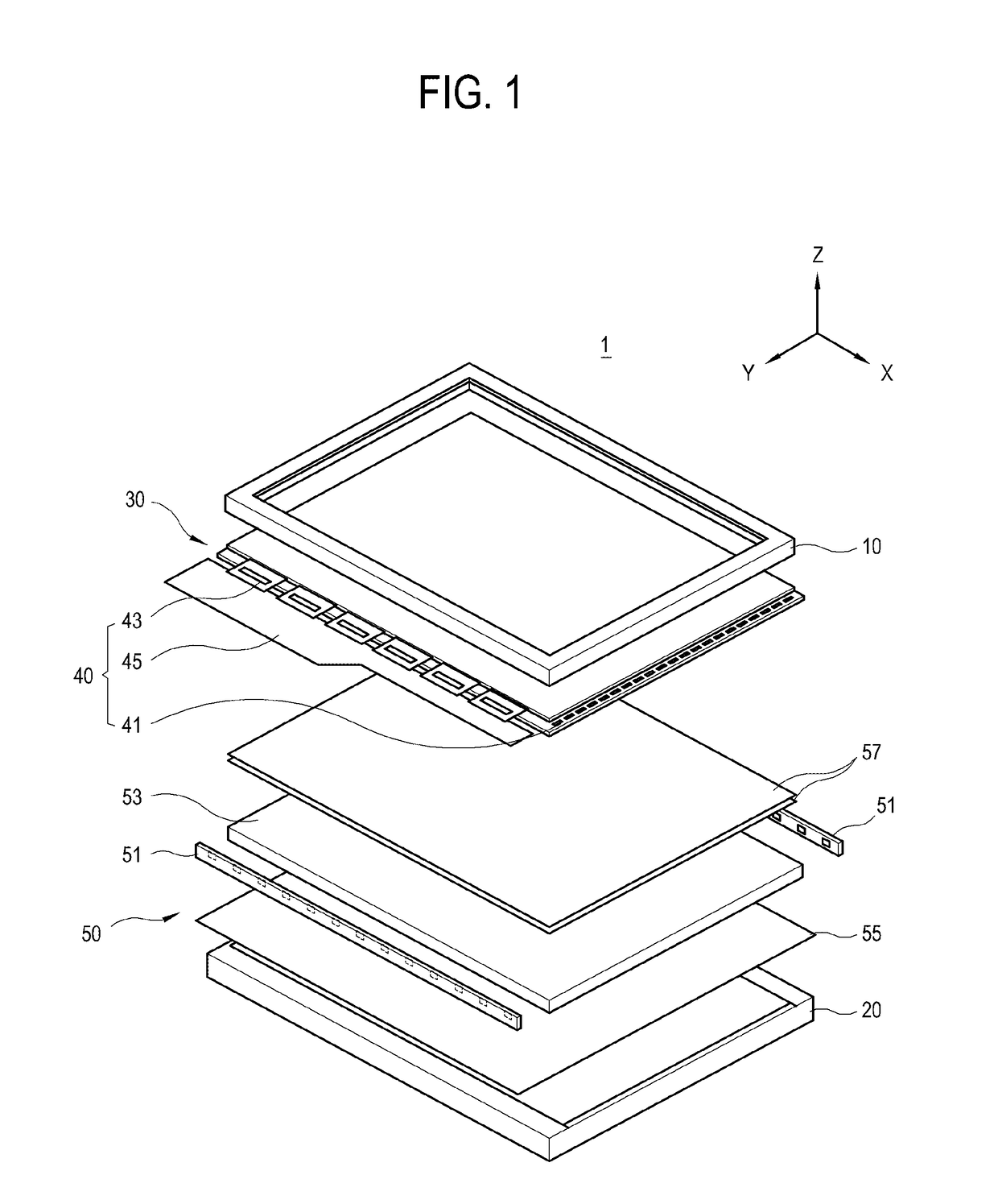
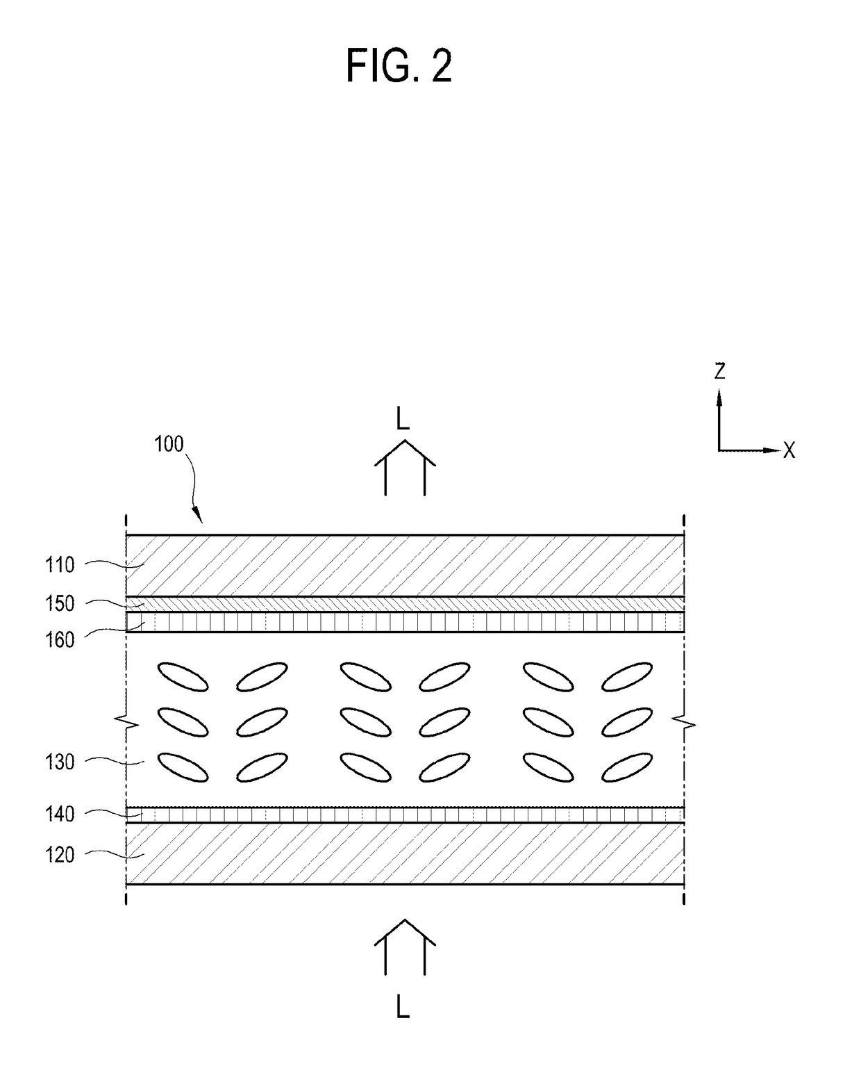
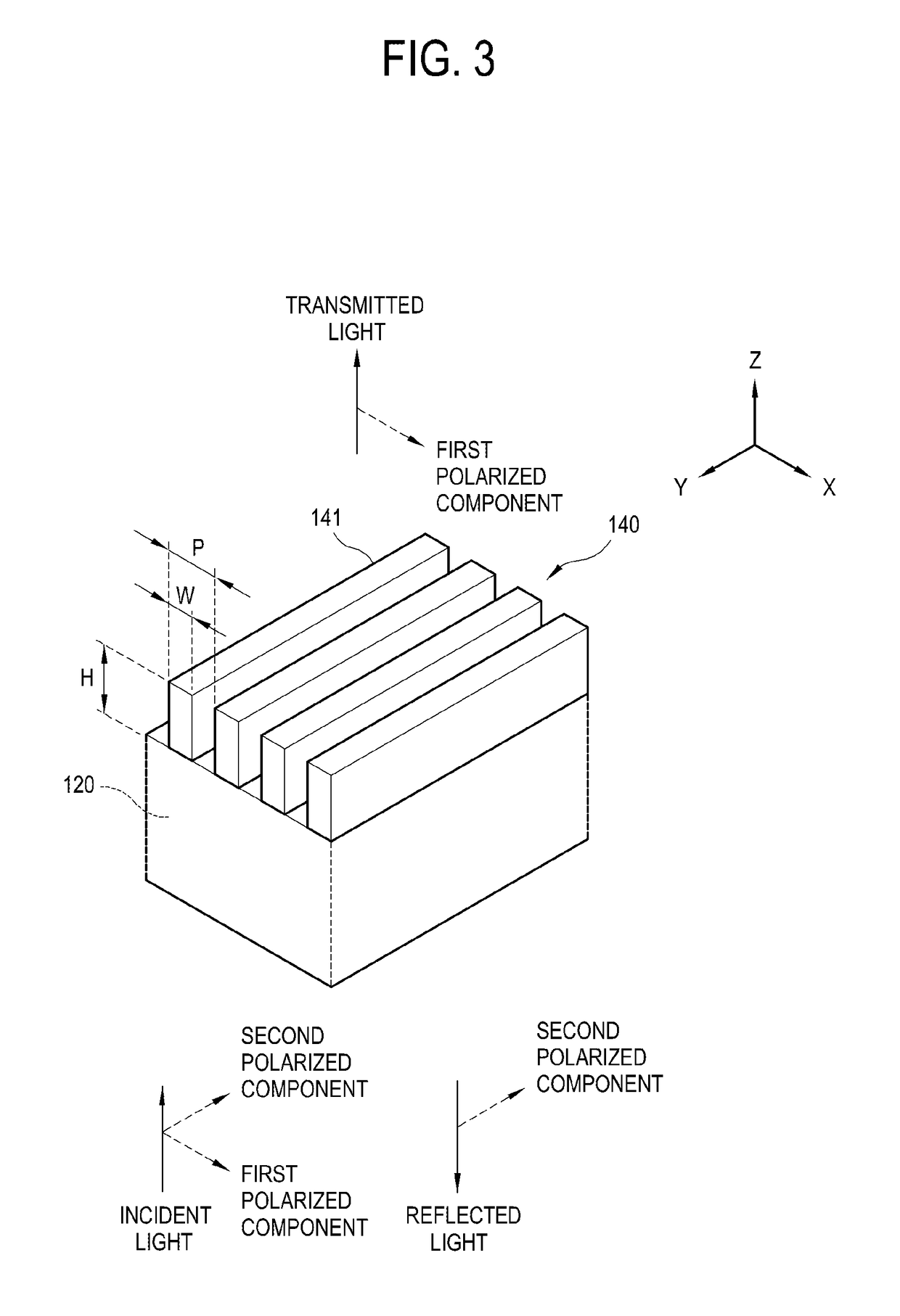
[0032]Below, example embodiments will be described in greater detail with reference to accompanying drawings. The following descriptions of the example embodiments are made by referring to elements shown in the accompanying drawings, in which like numerals refer to like elements having substantively the same functions.

[0033]In the description of the example embodiments, an ordinal number used in terms such as a first element, a second element, etc. is employed for describing variety of elements, and the terms are used for distinguishing between one element and another element. Therefore, the meanings of the elements are not limited by the terms, and the terms are also used simply for explaining the corresponding example without limiting the disclosure.

[0034]Further, the example embodiments will describe only elements directly related to the disclosure, and a description of other elements may be omitted. However, it will be appreciated that the elements, the descriptions of which are...


PUM

PropertyMeasurementUnit
diagonal lengthaaaaaaaaaa
areaaaaaaaaaaa
heightaaaaaaaaaa

Abstract

A method of manufacturing a linear grid on a substrate to form a linear grid pattern of a display panel, the method including: laminating a negative photoresist layer having a linear grid pattern on a first area of a substrate, said substrate including a pattern forming layer disposed thereon; laminating a positive photoresist layer having a linear grid pattern on a second area of the substrate and overlapping at least a portion of the negative photoresist layer of the first area; covering the second area with a mask and exposing the first area; and forming a linear grid pattern by removing the mask and etching the pattern forming layer.

Description

CROSS-REFERENCE TO RELATED APPLICATION[0001]This application is based on and claims priority under 35 U.S.C. § 119 to Korean Patent Application No. 10-2015-0020852, filed on Feb. 11, 2015 in the Korean Intellectual Property Office, the disclosure of which is incorporated by reference herein in its entirety.BACKGROUND[0002]Field[0003]Apparatuses and methods relate generally to a method of manufacturing a linear grid for a substrate to form a linear-grid structure on a substrate of various display panels, and a mold and display apparatus manufactured by the same, and for example, to a method of manufacturing a linear grid for a substrate, in which a manufacturing fault such as a seam line is minimized or reduced when a master mold corresponding to the linear grid formed on the substrate for a large screen is manufactured, and a mold and display apparatus manufactured by the same.[0004]Related Art[0005]A display apparatus includes a display panel for displaying an image based on a broa...

Claims


Application Information

Patent Timeline
Patent Type & Authority Patents(United States)
IPC IPC(8): H01L21/469G02F1/1335G03F7/00G02B5/30
CPCG02F1/133528G02B5/3025G03F7/0002G02F1/133536G02F2001/133548G02F1/133548G02F1/1333G02F1/13625
Inventor KIM, DONG-HWAN
Owner SAMSUNG ELECTRONICS CO LTD
Why Eureka
Try Eureka