
Nano bi-material electromagnetic spectrum shifter

a bi-material and electromagnetic spectrum technology, applied in the direction of instruments, optical elements, vacuum evaporation coating, etc., can solve the problems of low transmission, single metal np can only produce color tuning, and precision multi-layer deposition that can be time-consuming in fabrication, so as to achieve color tunability and widen the transmission range

Active Publication Date: 2019-01-29
HONG KONG BAPTIST UNIV
View PDF1 Cites 0 Cited by
  • Summary
  • Abstract
  • Description
  • Claims
  • Application Information

AI Technical Summary

Benefits of technology

[0009]It is an objective of the present invention is to produce a nano bi-material for electromagnetic spectrum shifter including color filters and reflectors to result in a wider transmission range and color tunability.
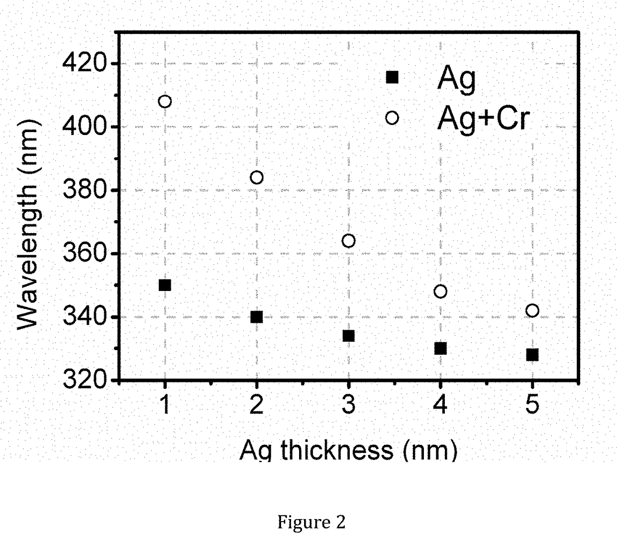
[0018]In a sixth embodiment of the third aspect of the present invention there is provided a tunable electromagnetic spectrum shifter wherein the one nano metal particles is composed of metals which are screened plasma frequency at near-ultraviolet region or visible spectral regions such that the resonance is tunable in the visible spectral region due to the red-shift phenomenon in the presence of said at least one other different nano particles which are brought to close proximity to the one nano metal particles, and have a relatively lower absorption in visible spectral region such that a relatively higher overall transmittance is resulted in said shifter.

Problems solved by technology

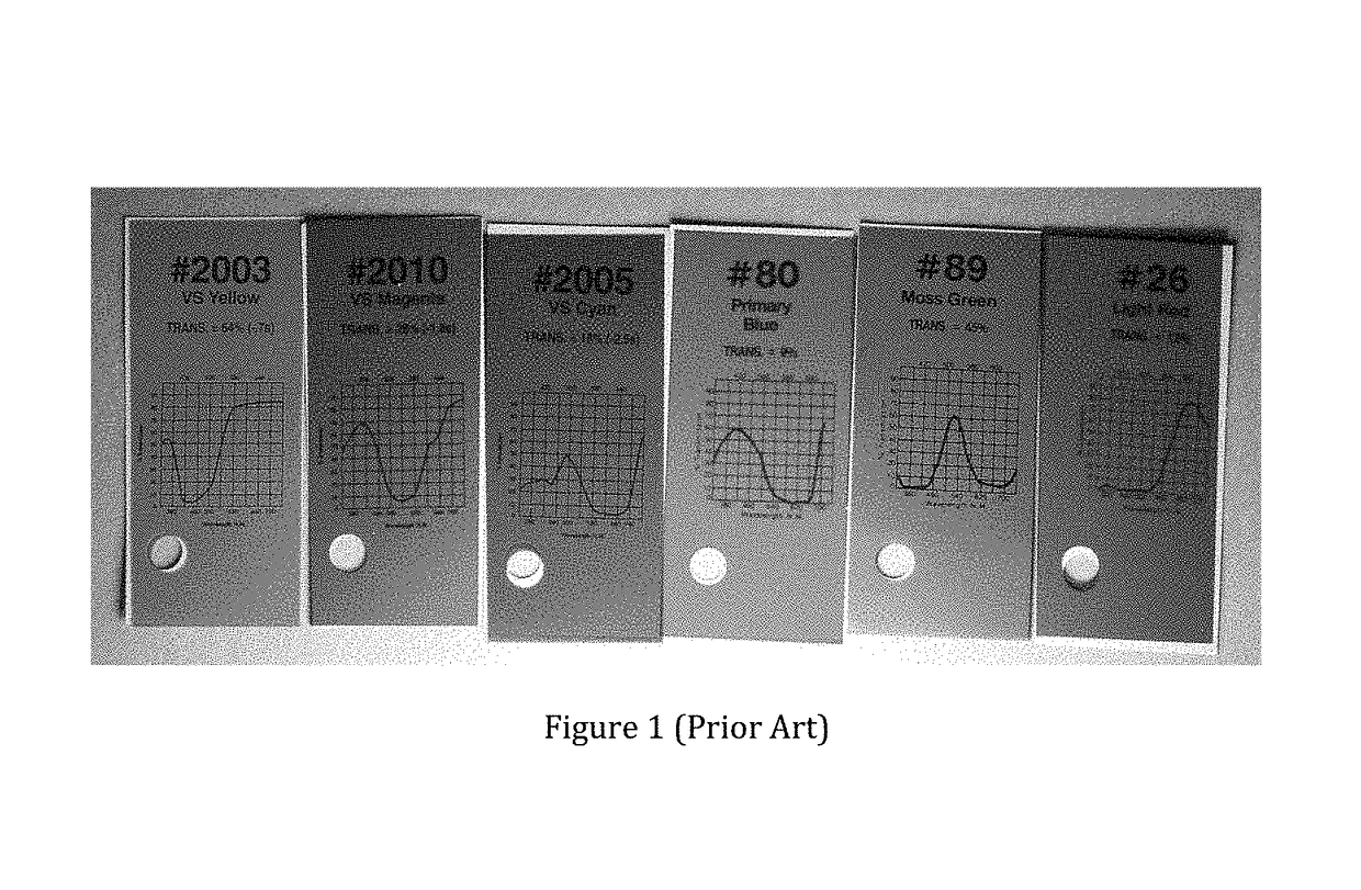
The former needs thick substrate to produce desired color effect but then causes low transmission (typically <40%), while the latter requires precision multi-layer deposition that can be time consuming in fabrication.
However using single metal NP can only produce color tuning by varying its dimension.
Hence, the tuning range is somewhat limited.

Method used


Image

  • Nano bi-material electromagnetic spectrum shifter
  • Nano bi-material electromagnetic spectrum shifter
  • Nano bi-material electromagnetic spectrum shifter

Examples


Embodiment Construction

[0067]The present invention is not to be limited in scope by any of the specific embodiments described herein. The following embodiments are presented for exemplification only.

[0068]Without wishing to be bound by theory, the inventors have discovered through their trials, experimentations and research that to accomplish the task of producing color filters as an example of electromagnetic spectrum shifter using nano bi-material and inventing said color filters using nano bi-material.

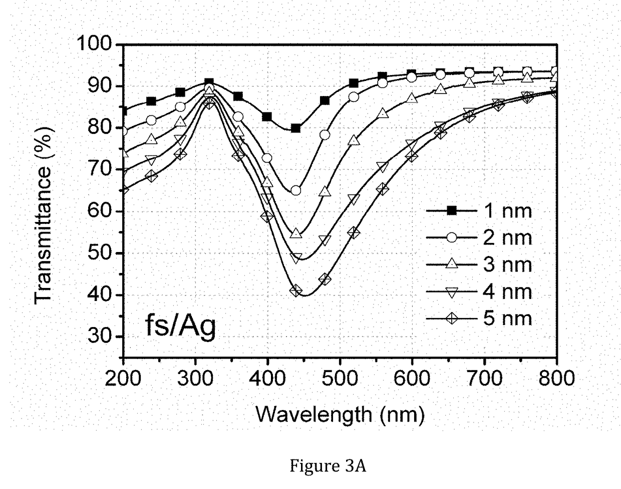
[0069]In one embodiment of the present invention. the following two parameters are the key features / solutions being provided: (i) dimension and / or number of metal nano particles (NPs) and (ii) plasmonic coupling of two dissimilar (or different) metal NPs to tune the color, leading to a rich range of color filter, e.g. violet, purple, blue, yellow, orange, pink, etc., hence, the color filters of the present invention have a wider range of transmission and color tunability. The dimension and number of metal...


PUM

PropertyMeasurementUnit
thicknessaaaaaaaaaa
thicknessaaaaaaaaaa
diameteraaaaaaaaaa

Abstract

The present invention relates to a nano bi-material, electromagnetic spectrum shifter based on said nano bi-material and method to produce said electromagnetic spectrum shifter using said nano bi-material. In particular, the present invention provides nano bi-material based electromagnetic spectrum shifter, e.g. color filters, with a wide range of transmission and color tunability and methods to produce said color filters. The present invention has applications in color filtration and production of color filters; reflector and production of reflectors; and electromagnetic spectrum shifter and production of electromagnetic spectrum shifters.

Description

CROSS-REFERENCE TO RELATED APPLICATIONS[0001]This application claims the benefit of U.S. Provisional Patent Application Ser. No. 62 / 234,662 filed Sep. 30, 2015; the disclosures of which are incorporated herein by reference in their entirety.FIELD OF THE INVENTION[0002]The present invention relates to a nano bi-material electromagnetic spectrum shifter based on said nano bi-material and method to produce such color filters using nano bi-material. Said nano bi-material comprises two materials, wherein at least one of said material is metal based. In particular, the present invention provides said nano bi-material based electromagnetic spectrum shifter with a wide range of transmission and color tunability and methods to produce such electromagnetic spectrum shifters.BACKGROUND OF THE INVENTION[0003]When light passes through a color filter, some color components are removed. This is known as color subtraction. For example, a magenta filter would remove the green color, leaving the blue...

Claims


Application Information

Patent Timeline
Patent Type & Authority Patents(United States)
IPC IPC(8): G02B5/22C23C14/18C03C17/09G02B1/14C23C14/20C03C17/38C03C17/36C03C17/00G02B5/08G02B5/00
CPCG02B5/22C03C17/09C03C17/36C03C17/3605C03C17/38C23C14/18C23C14/20G02B1/14G02B5/008G02B5/0808C03C17/007C03C2218/151C03C2217/252C03C2217/253C03C2217/256C03C2217/258C03C2217/26C03C2217/445C03C2217/45C03C2217/479
Inventor CHEAH, KOK WAICHING, SUET YING
Owner HONG KONG BAPTIST UNIV
Learn More