Optical film laminate used for continuous lamination to panel component

a technology of optical film laminate and panel component, applied in the direction of instruments, polarising elements, other domestic objects, etc., can solve the problems of inductive electrification, inability to avoid the effect of carrier film, and deterioration of static electricity of electrified optical display devices

Inactive Publication Date: 2019-02-05
NITTO DENKO CORP
View PDF44 Cites 0 Cited by
  • Summary
  • Abstract
  • Description
  • Claims
  • Application Information

AI Technical Summary

Benefits of technology

[0021]An aim of the present invention is to provide a continuous web of optical film laminate which may promptly attenuate static electrification caused by peeling in both of the optical film laminate and a releasable film in RTP lamination method and apparatus for continuously manufacturing optical display devices by laminating optical film sheets to panel components.

Problems solved by technology

It has been well known that static electricity of electrified optical display device can deteriorate or can even damage built-in electronic components.
Thus, a remaining problem is how to attenuate static charge of a polarizing film sheet including an adhesive layer statically electrified by peeling, before laminating to a liquid crystal panel.
More in particular, in RTP lamination method and apparatus, since a liquid crystal panel is conveyed to a predetermined lamination position in close vicinity of a peeled carrier film where a polarizing film sheet including an adhesive layer is laminated to the liquid crystal panel while being peeled from the carrier film, it is not possible to avoid effect of the carrier film and the polarizing film sheet that are statically electrified by peeling.
That is, at least two problems need to be solved to prevent static electrification of a liquid crystal panel in RTP lamination method and apparatus.
A first problem is to prevent inductive electrification of a liquid crystal panel induced by a carrier film, being conveyed in close vicinity of the carrier film which is statically electrified by peeling.
A second problem is how to address inductive electrification of the liquid crystal panel caused when laminating thereto a polarizing film sheet including an adhesive layer which is statically electrified while peeling from the carrier film.
If it is addressed incompletely, electronic components built-in an inductively-electrified liquid crystal panel may be damaged by static electricity, or even if not damaged, light leaking parts due to orientation disorder of liquid crystal may be found in an inspection process in a completed liquid crystal display device, as seen in a photograph in FIG. 2.
As a result, a transmission inspection of a liquid crystal display device as a product becomes difficult which in turn compromises continuous manufacturing of a liquid crystal display device.

Method used


Image

  • Optical film laminate used for continuous lamination to panel component
  • Optical film laminate used for continuous lamination to panel component
  • Optical film laminate used for continuous lamination to panel component

Examples


Embodiment Construction

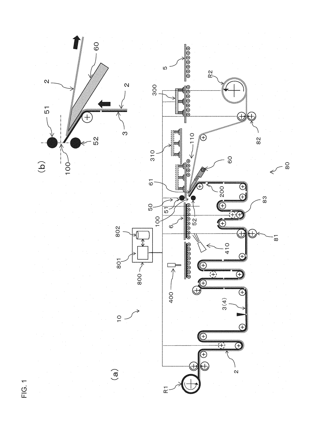
[0043]FIG. 1 (a) is a schematic diagram showing an entire RTP lamination apparatus. In the RTP lamination apparatus 10, a continuous web of optical film laminate 1 is wound on a feeding roller R1. The optical film laminate 1 comprises a carrier film 2 having a width corresponding at least to a size (a long side or a short side) of a panel component 5 and a plurality of optical film sheets 3 continuously supported on an adhesive layer 4 formed on one of surfaces of the carrier film 2. The optical film sheets 3 are formed on a film sheet including the adhesive layer 4 by forming slit lines reaching to a surface of the carrier film 2 in an optical film laminated via the adhesive layer 4 to the carrier film 2 with intervals corresponding to a size (a short side or a long side) of the panel component 5.

[0044]The RTP lamination apparatus 10 comprises a film feeding apparatus 80 consisting of up-stream rollers 81 for feeding the optical film laminate 1 from the feed roller R1 and down-stre...


PUM

PropertyMeasurementUnit
conductiveaaaaaaaaaa
sheet resistanceaaaaaaaaaa
widthaaaaaaaaaa

Abstract

To provide a continuous web of optical film laminate provided with static electrification prevention function which allows for promptly attenuating static charge of optical film sheet and carrier film electrified by peeling action in RTP lamination method and apparatus. The problem has been solved with a continuous web of optical film laminate for using in RTP lamination method and apparatus, in which static electrification prevention function is provided to optical film sheets and a carrier film configuring the continuous web of optical film laminate, such that sheet resistance of each of the optical film sheets and the carrier film is 1012 Ω / sq or less so as to promptly attenuate static charge of the carrier film to be collected, which is statically electrified by peeling action, and the optical film sheets to be laminated to panel components, which are also statically electrified by peeling action.

Description

CROSS REFERENCE TO RELATED APPLICATION[0001]This application claims the priority of Japanese Patent Application No. 2015-060266, filed on Mar. 24, 2015 in the Japanese Patent Office. Further, this application is the National Phase application of International Application No. PCT / JP2015 / 080979 filed on Nov. 4, 2015, which is incorporated herein by reference in its entirety.TECHNICAL FIELD[0002]The present invention relates to a continuous web of optical film laminate to be used in a method and an apparatus for continuously manufacturing optical display devices by laminating optical film sheets to panel components (hereinafter referred as “RTP lamination method and apparatus”).[0003]More in particular, in RTP lamination method and apparatus for continuously manufacturing optical display devices by laminating optical film sheets via adhesive layer to panel components conveyed to a predetermined lamination position, when a carrier film which is laminated to an adhesive layer and configu...

Claims


Application Information

Patent Timeline
Patent Type & Authority Patents(United States)
IPC IPC(8): G02B1/16B32B27/00G02F1/1335B32B7/02C08J7/04G02B5/30G02B1/14B32B7/12G02F1/13C08J7/043C08J7/044
CPCG02B1/16B32B27/00C08J7/045G02B1/14G02B5/305G02B5/3033G02F1/1335G02F1/133528B32B7/02Y10T428/1055B32B7/12B32B2307/40B32B2457/202G02F1/1303G02F2202/22G02F2202/28C09K2323/04C08J7/043C08J7/044C08J7/0423
Inventor MORIMOTO, YUTOYAMA, YUSUKEISHII, TAKAAKIKITADA, KAZUOHASHIMOTONAGURA, AKIHIRO
Owner NITTO DENKO CORP
Why Eureka
Try Eureka