

Substrate structure and manufacturing method thereof
a technology of substrate structure and manufacturing method, which is applied in the direction of printed circuit manufacturing, cross-talk/noise/interference reduction, circuit electrical arrangement, etc., can solve the problems of complex circuit layout, complex process, complex material, and higher cost, and achieve low cost and high electric
- Summary
- Abstract
- Description
- Claims
- Application Information
AI Technical Summary
Benefits of technology
Problems solved by technology
Method used
Image

Examples
first embodiment
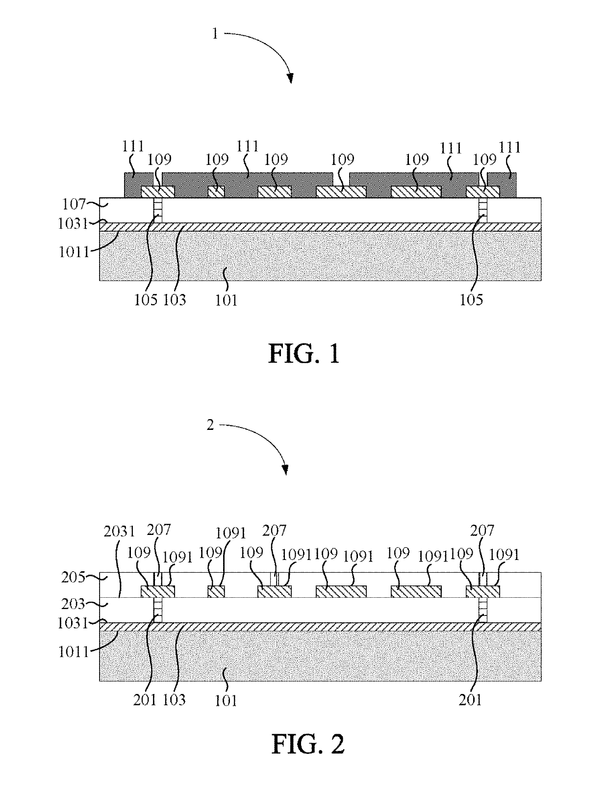
[0025]Referring to FIG. 1, a substrate structure 1 includes a metal carrier 101, a first conductive wiring layer 103, a conductive pillar layer 105, a dielectric material layer 107, a second conductive wiring layer 109 and a protective layer 111. The conductive pillar layer 105 has a plurality of conductive pillars. The dielectric material layer 107 is a molding compound layer having Novolac-based Resin, Epoxy-based Resin, Silicone-based Resin or other suitable material. In the embodiment, the conductive pillar layer 105 has two conductive pillars.
[0026]The metal carrier 101 has a surface 1011. The first conductive wiring layer 103 has a surface 1031. The first conductive wiring layer 103 is disposed on the surface 1011 of the metal carrier 101. The dielectric material layer 107 is disposed on the surface 1031 of the first conductive wiring layer 103. The second conductive wiring layer 109 is disposed on the dielectric material layer 107 that is partially covering the dielectric ma...
fourth embodiment
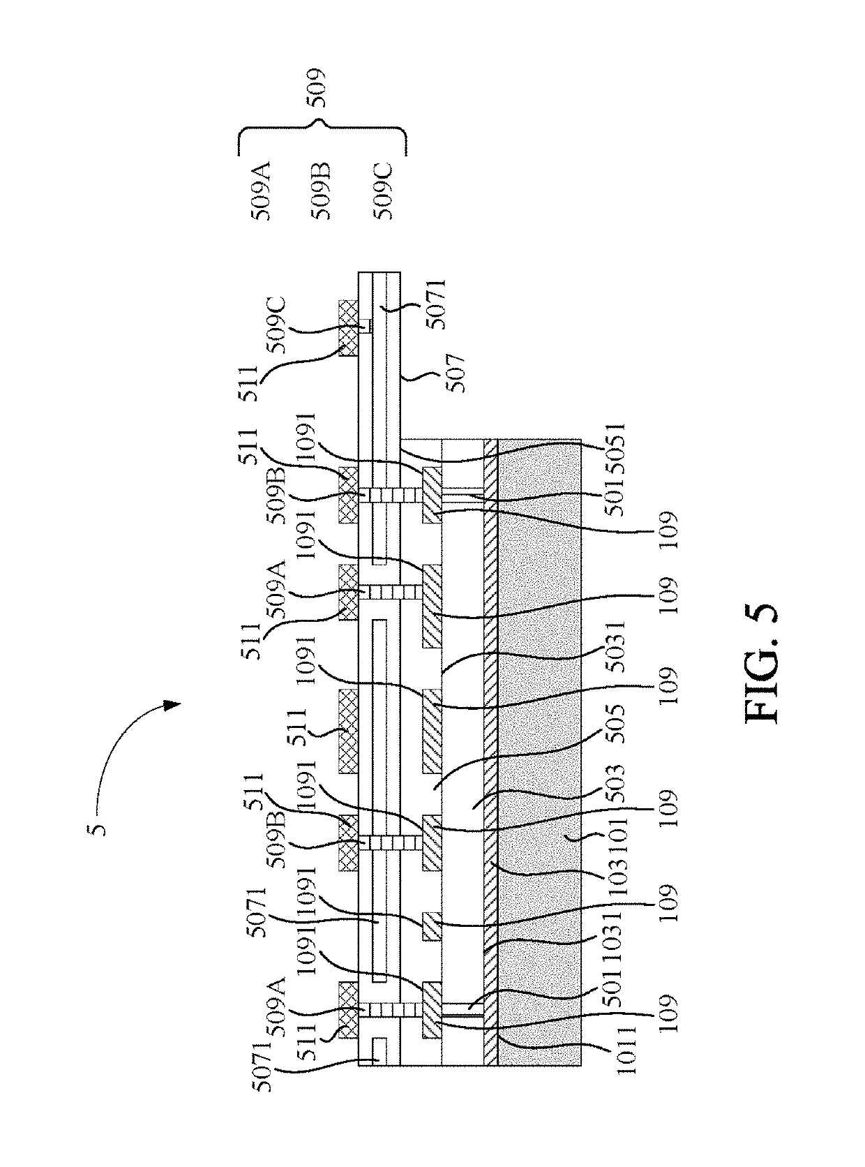
[0035]The third dielectric material layer 401 is a molding compound layer having Novolac-based Resin, Epoxy-based Resin, Silicone-based Resin or other suitable material. In the fourth embodiment, the third conductive pillar layer 403 has four conductive pillars.
[0036]The third conductive wiring layer 301 has a surface 3011. The third dielectric material layer 401 is disposed on the surface 3011 of the third conductive wiring layer 301 and the surface 2051 of the second dielectric material layer 205. The third conductive pillar layer 403 is disposed inside the third dielectric material layer 401 and electrically connected to the third conductive wiring layer 301. More detailed, at least one of the conductive pillars of the third conductive pillar layer 403 has a first end and a second end, which is opposite to the first end. The first end of the conductive pillar of the third conductive pillar layer 403 is electrically connected to the third conductive wiring layer 301. The second en...
fifth embodiment
[0038]The first dielectric material layer 503 and the second dielectric material layer 505 are a molding compound layer, respectively, that has Novolac-based Resin, Epoxy-based Resin, Silicone-based Resin or other suitable material, respectively. In the fifth embodiment, the first conductive pillar layer 501 has two conductive pillars and the second conductive pillar layer 509 has five conductive pillars 509A, 509B and 509C.
[0039]The first dielectric material layer 503 has a surface 5031. The second conductive wiring layer 109 has a surface 1091. The second dielectric material layer 505 has a surface 5051. The flexible circuit board 507 has a conductive wiring layer 5071. The second dielectric material layer 505 is disposed on the surface 1091 of the second conductive wiring layer 109 and the surface 5031 of the first dielectric material layer 503. The third conductive wiring layer 511 is disposed on the flexible circuit board 507. The second conductive pillar layer 509 is disposed ...
PUM
 Abstract
Description
Claims
Application Information