
Biometric device and method thereof and wearable carrier

a biometric device and wearable technology, applied in the field of recognition devices and methods thereof, can solve the problems of large power consumption of the whole image capturing operation, large data amount of images, and very slow processing speed, and achieve the effect of thinning

Active Publication Date: 2020-02-06
IND TECH RES INST
View PDF35 Cites 0 Cited by
  • Summary
  • Abstract
  • Description
  • Claims
  • Application Information

AI Technical Summary

Benefits of technology

The patent is about a biometric method that uses a thinner and more efficient design to process data faster. The method involves sequentially lighting infrared light emitting diodes to decrease the amount of data needed to be processed, allowing for quicker image processing. The design also includes an optical layer with a lens portion that creates a planar light source, reducing power consumption. Overall, the method and device provide a thinner, faster, and more efficient way to perform biometric recognition.

Problems solved by technology

Moreover, taking finger, palm vein recognition as an example, a vein image is generally captured first, and regarding the current technique, a data amount of the image is relatively large, a processing speed thereof is very slow, and power consumption of the whole image capturing operation is relatively large, which is not suitable for ID recognition of the smart wearable device.
Therefore, how to design a biometric device with low power consumption, thinned modules and a fast processing speed has become an important technical challenge in design of the biometric device.

Method used


Image

  • Biometric device and method thereof and wearable carrier
  • Biometric device and method thereof and wearable carrier
  • Biometric device and method thereof and wearable carrier

Examples


Embodiment Construction

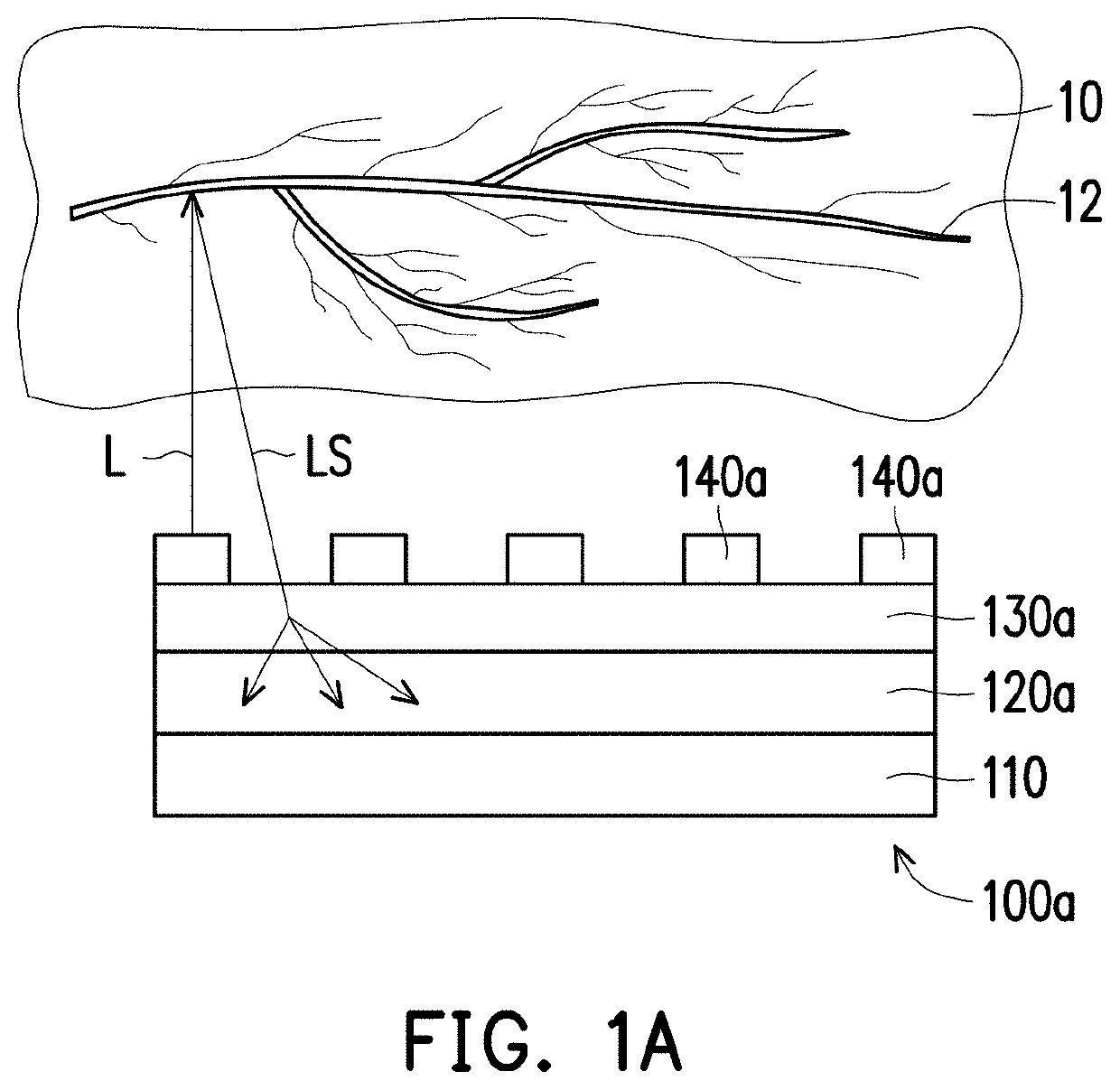
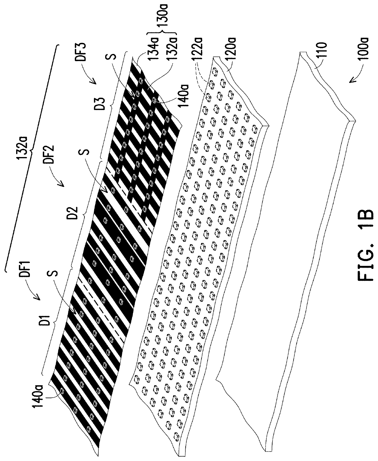
[0032]FIG. 1A is a cross-sectional view of a biometric device according to an embodiment of the disclosure. FIG. 1B is a partial top view of an exploded schematic diagram of the biometric device of FIG. 1A. Referring to FIG. 1A and FIG. 1B, in the present embodiment, the biometric device 100a is adapted to recognize a biological characteristic of a region 12 of a biological body 10, where the region 12 of the biological body 10 is, for example, a wrist of a human body, and the biological characteristic is, for example, a vein network image characteristic. The biometric device 100a includes a substrate 110, an image sensor 120a, an optical layer 130a and at least one infrared light emitting diode (IR LED) 140a (in FIG. 1A and FIG. 1B, a plurality of IR LEDs is schematically illustrated). The image sensor 120a is disposed on the substrate 110. The optical layer 130a is disposed on the image sensor 120a and includes a diffraction pattern 132a. The IR LEDs 140a are disposed on the diffr...


PUM

PropertyMeasurementUnit
reflectivityaaaaaaaaaa
transparentaaaaaaaaaa
poweraaaaaaaaaa

Abstract

A biometric device includes a substrate, an image sensor, an optical layer and at least one infrared light emitting diode (IR LED). The image sensor is disposed on the substrate. The optical layer is disposed on the image sensor and includes a diffraction pattern. The IR LED is disposed on the diffraction pattern of the optical layer. The optical layer is located between the IR LED and the image sensor.

Description

CROSS-REFERENCE TO RELATED APPLICATION[0001]This application is a continuation application of and claims the priority benefit of a prior U.S. application Ser. No. 15 / 221,615, filed on Jul. 28, 2016, now pending. The prior U.S. application Ser. No. 15 / 221,615 claims the priority benefits of U.S. provisional application Ser. No. 62 / 198,645, filed on Jul. 29, 2015 and Taiwan application serial no. 105120683, filed on Jun. 30, 2016. The entirety of each of the above-mentioned patent applications is hereby incorporated by reference herein and made a part of this specification.BACKGROUND OF THE DISCLOSUREField of the Disclosure[0002]The disclosure relates to a recognition device and a method thereof, and particularly relates to a biometric device and a method thereof and a wearable carrier using the biometric device.Description of Related Art[0003]Biometrics plays a more and more important role in today's society, where types of the biometrics mainly include face recognition, iris recogni...

Claims


Application Information

Patent Timeline
Patent Type & Authority Applications(United States)
IPC IPC(8): G06K9/00H04N5/33G06V10/143G06V10/147
CPCH04N5/33G06K2009/00932H04N5/2256G06K9/00885G06V40/10G06V40/14G06V10/17G06V10/143G06V10/147H04N23/56
Inventor CHAO, CHIA-HSINFANG, YEN-HSIANGWU, MING-HSIEN
Owner IND TECH RES INST
Learn More