Antenna matching circuit, antenna device, and communication terminal apparatus

a technology of antenna devices and matching circuits, applied in the direction of electrical devices, multiple-port networks, transmission, etc., can solve the problems of inability to achieve high-band matching, and inability to achieve impedance matching over a wide band. , to achieve the effect of reducing the number of components to be mounted on the substrate, reducing the cost and easy disassembly

Active Publication Date: 2019-07-02
MURATA MFG CO LTD
View PDF14 Cites 0 Cited by
  • Summary
  • Abstract
  • Description
  • Claims
  • Application Information

AI Technical Summary

Benefits of technology

[0011]With this configuration, the impedance conversion ratio in the high band is maintained to be relatively small, and the impedance conversion performed by the transformer operates effectively in the low band (without changing the characteristics of the antenna in the high band).
[0013]In an antenna matching circuit according to a preferred embodiment of the present invention, it is preferable that the antenna matching circuit further includes a substrate on which a transmission line that leads to the antenna port is provided. It is also preferable that the impedance converter circuit be a chip component defined by a single multilayer body including a plurality of base material layers that are laminated, the first inductance element and the second inductance element be provided in an interior of the multilayer body, signal input / output terminals be provided on two sides, facing each other, of the multilayer body, and the impedance converter circuit, the third inductance element, and the capacitance element be provided on the substrate. Accordingly, the antenna matching circuit is able to be easily disposed in a middle portion of the linear transmission line between the feeder circuit and the antenna. The impedance converter circuit and the impedance-conversion-ratio adjustment circuit are able to be provided in a little space on the substrate.
[0014]In an antenna matching circuit according to a preferred embodiment of the present invention, the third inductance element may preferably be a portion of a signal line of the transmission line. Accordingly, the number of components to be mounted on the substrate is reduced so as to reduce the cost.

Problems solved by technology

As described above, if such an impedance converter circuit is applied to an antenna whose impedance has large frequency dependence, it is difficult to achieve impedance matching over a wide band.
That is, because the impedance conversion ratio becomes too great in the high band, matching is not achieved in a portion of the high band.
However, the effect of adjusting the frequency characteristics of the impedance conversion ratio is small even when the RF path is provided in a transformer whose coils have very small inductance.

Method used


Image

  • Antenna matching circuit, antenna device, and communication terminal apparatus
  • Antenna matching circuit, antenna device, and communication terminal apparatus
  • Antenna matching circuit, antenna device, and communication terminal apparatus

Examples


first preferred embodiment

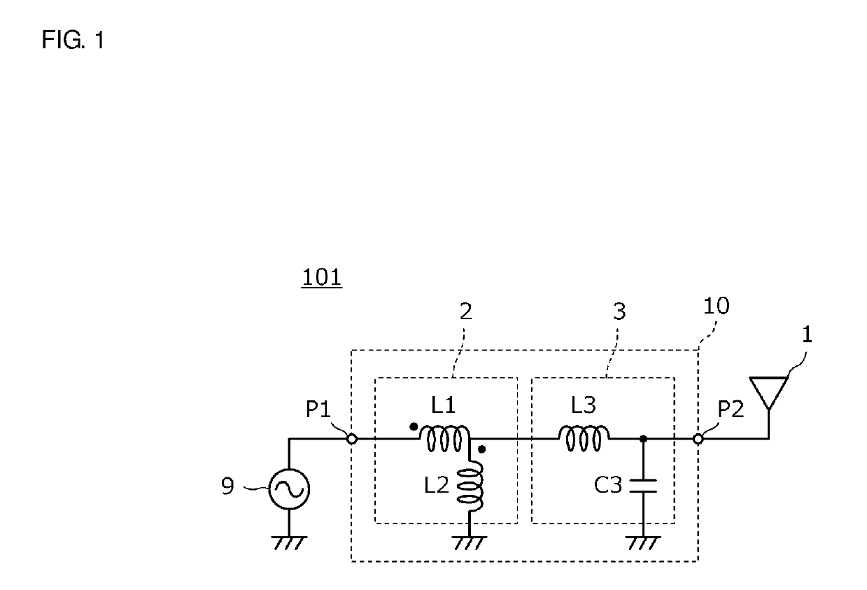
[0038]FIG. 1 is a circuit diagram illustrating the configuration of an antenna matching circuit and an antenna device according to a first preferred embodiment of the present invention. An antenna device 101 includes an antenna 1, a feeder circuit 9, and an antenna matching circuit 10. The antenna matching circuit 10 is connected between the antenna 1 and the feeder circuit 9.

[0039]The antenna matching circuit 10 includes an impedance converter circuit 2 and an impedance-conversion-ratio adjustment circuit 3.

[0040]The impedance converter circuit 2 includes a first inductance element L1 and a second inductance element L2, which are coupled to each other through magnetic fields. A first end of the first inductance element L1 is connected to the feeder circuit 9; a first end of the second inductance element L2 is connected to a second end of the first inductance element L1; and a second end of the second inductance element L2 is connected to ground. The first inductance element L1 and ...

second preferred embodiment

[0057]A second preferred embodiment of the present invention provides an antenna matching circuit element 10P where the antenna matching circuit 10 discussed in the first preferred embodiment is a single component.

[0058]FIG. 6 is an exploded perspective view of the antenna matching circuit element 10P according to the second preferred embodiment.

[0059]The antenna matching circuit element 10P includes a plurality of insulating base material layers 11 to 24. Various conductor patterns are provided on the base material layers 11 to 24. The “various conductor patterns” preferably include not only conductor patterns provided on the surface of the base material layers, but also inter-layer connection conductors, for example. The inter-layer connection conductors preferably include not only via conductors, but also end-surface electrodes provided on the end surfaces of a multilayer body. The antenna matching circuit element 10P is preferably a multilayer body including the base material la...

third preferred embodiment

[0070]FIG. 9 is a plan view illustrating the structure of an antenna device 103 of a third preferred embodiment of the present invention. A transmission line with a coplanar line structure includes ground conductors GND and a signal line SL on a substrate 20. The antenna 1 and the feeder circuit 9 are connected to the transmission line. The circuit configuration of the antenna device 103 is preferably the same as or similar to the antenna device 101 discussed in the first preferred embodiment.

[0071]The impedance converter circuit 2 is preferably a surface-mountable chip component. The third inductance element L3 and the capacitance element C3 are both chip components. The antenna device 103 is configured by mounting the impedance converter circuit 2, the third inductance element L3, and the capacitance element C3 on the substrate 20.

[0072]The impedance converter circuit 2 is preferably provided in a single rectangular or substantially rectangular parallelepiped multilayer body inclu...


PUM


Abstract

An antenna device includes an impedance converter circuit connected to a feeder circuit, an impedance-conversion-ratio adjustment circuit, and an antenna. The impedance converter circuit includes a first inductance element and a second inductance element, which are coupled to each other through magnetic fields, so as to provide an autotransformer circuit. The impedance-conversion-ratio adjustment circuit includes a third inductance element which is series-connected between the impedance converter circuit and an antenna port, and a capacitance element which is shunt-connected between the antenna port and ground. The impedance-conversion-ratio adjustment circuit corrects an impedance conversion ratio of the impedance converter circuit in accordance with a frequency band.

Description

CROSS REFERENCE TO RELATED APPLICATIONS[0001]This application claims the benefit of priority to Japanese Patent Application No. 2015-006665 filed on Jan. 16, 2015 and is a Continuation Application of PCT Application No. PCT / JP2016 / 050184 filed on Jan. 6, 2016. The entire contents of each application are hereby incorporated herein by reference.BACKGROUND OF THE INVENTION1. Field of the Invention[0002]The present invention relates to an antenna matching circuit connected between an antenna and a feeder circuit, an antenna device including the antenna matching circuit, and a communication terminal apparatus including the antenna device.2. Description of the Related Art[0003]In recent years, to cope with the widening of a frequency band required for communication terminal apparatuses, such as cellular phones, an impedance converter circuit including a transformer has been used in an antenna matching circuit, as discussed in, for example, International Publication No. 2012 / 153691. Meanwh...

Claims


Application Information

Patent Timeline
Patent Type & Authority Patents(United States)
IPC IPC(8): H01Q1/24H03H7/38H04B1/04H04B1/18H04B1/40H03H7/09H03H1/00
CPCH03H7/38H01Q1/24H03H7/09H04B1/0458H04B1/18H04B1/40H04B1/04H03H2001/0085
Inventor ISHIZUKA, KENICHI
Owner MURATA MFG CO LTD
Why Eureka
Try Eureka