Mechanism for preventing ESD damage and LCD panel utilizing the same

a technology of esd protection and mechanism, which is applied in the direction of static indicating devices, emergency protective arrangements for limiting excess voltage/current, instruments, etc., can solve the problems of reducing the yield and damage to internal elements, and the effectiveness of the protection offered by the esd protection device is not maintained, so as to prevent esd damage, reduce impedance, and the effect of reducing the width of the equivalent channel

Active Publication Date: 2007-10-09
AU OPTRONICS CORP
View PDF6 Cites 6 Cited by
  • Summary
  • Abstract
  • Description
  • Claims
  • Application Information

AI Technical Summary

Benefits of technology

[0007]Accordingly, an object of the present invention is to provide a mechanism for preventing ESD damage in an electronic device, such as an LCD panel. The ESD protection devices corresponding to the longest fan-out signal lines of an integrated circuit have substantially longer equivalent channel widths than those of the other ESD protection devices or substantially smaller impedances than those of the other ESD protection devices.
[0008]Another object of the invention is to provide a mechanism for preventing ESD damage in an electronic device, such as an LCD panel. The ESD protection devices corresponding to the outermost sides of the connection area have the substantially smallest impedance and impedances of the other ESD protection devices gradually increase from the outermost sides of the connection area to the substantially center thereof, thereby discharging the electrostatic charge efficiently.
[0009]Another object of the invention is to provide a mechanism for preventing ESD damage in an electronic device, such as an LCD panel. Any ESD protection device corresponding to one fan-out signal line of an integrated circuit has an impedance substantially different from impedances of the other ESD protection devices, thereby discharging the electrostatic charge efficiently.
[0010]Another object of the invention is to provide an liquid crystal display panel utilizing the above mechanism for preventing ESD damages, thereby preventing the LCD panel from damaged by ESD.

Problems solved by technology

When a machine or operator generates and transmits electrostatic discharge (ESD) to the TFT LCD panel, signal lines of the TFT LCD panel are open or short, resulting in reduced yield and damage to internal elements.
Therefore, the electrostatic charges do not disperse and the effectiveness of the protection offered by the ESD protection device is not maintained.

Method used


Image

  • Mechanism for preventing ESD damage and LCD panel utilizing the same
  • Mechanism for preventing ESD damage and LCD panel utilizing the same
  • Mechanism for preventing ESD damage and LCD panel utilizing the same

Examples


first embodiment

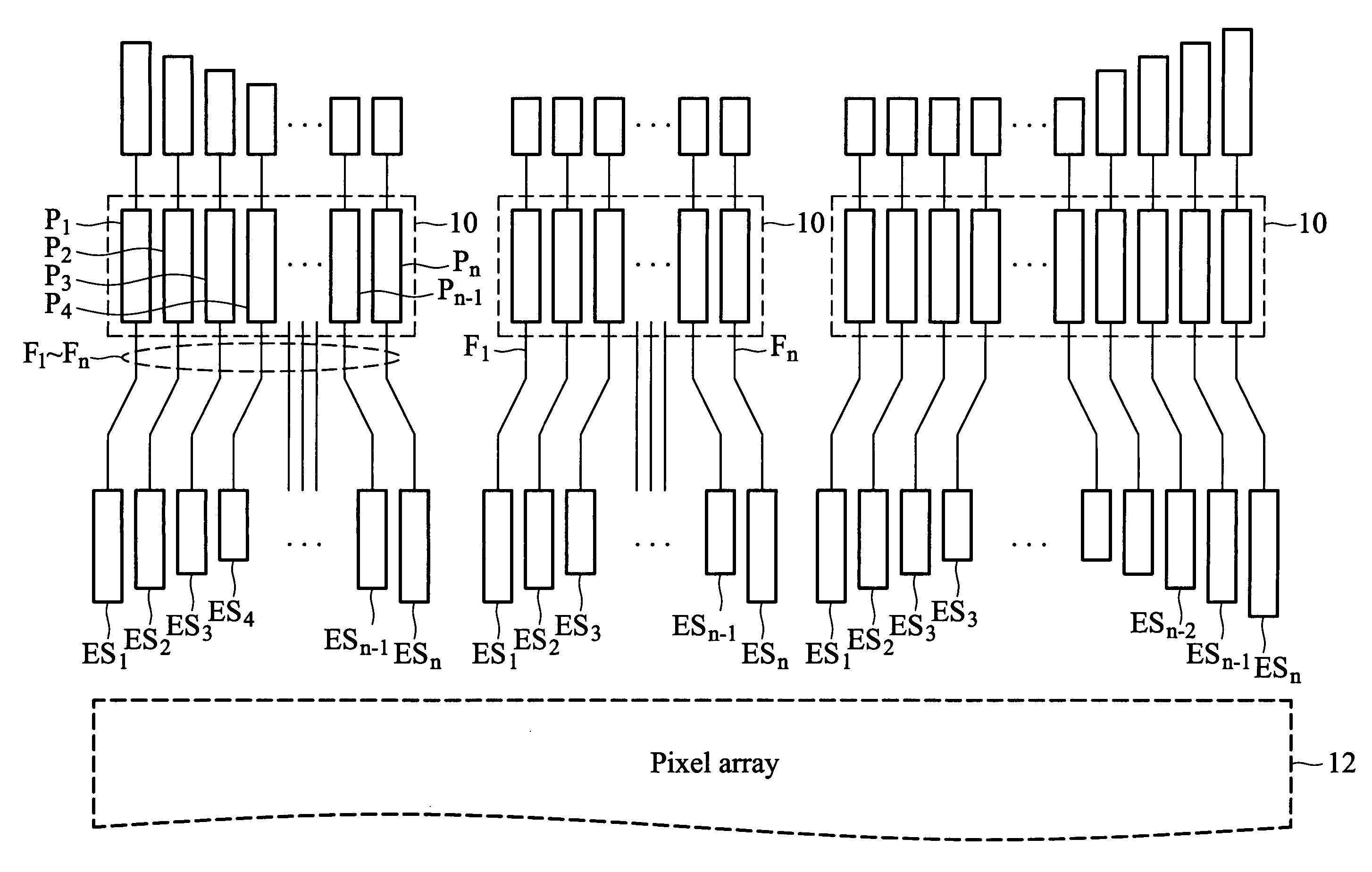
[0020]FIG. 4 shows an embodiment of a mechanism for preventing ESD damage in the present invention. The mechanism is applied to an electronic device, LCD panel.

[0021]The LCD panel comprises a pixel array 12, a plurality of connection areas 10, a plurality of fan-out signal lines F1 to Fn, and a plurality of ESD protection devices ES1 to EDn. Each connection area 10 has a plurality of pads P1 to Pn arranged sequentially for mounting to one integrated circuit. The pads P1 to Pn are disposed on two outermost sides of the connection area 10. The fan-out signal lines F1 to Fn extend from the pads P1 to Pn respectively. The ESD protection devices ES1 to EDn are disposed corresponding to the fan-out signal lines F1 to Fn. In addition, each ESD protection device comprises a least one element having a MOS transistor circuit structure, such as a MOS transistor whose drain is coupled to its gate.

[0022]As shown in FIG. 4, impedances of the ESD protection devices ES1 and EDn are designed to be s...

second embodiment

[0024]FIG. 5 shows another embodiment of a mechanism for preventing ESD damages in the present invention. The mechanism is applied to an electronic device, an LCD panel.

[0025]The LCD panel comprises a pixel array 12, a plurality of connection areas 10, a plurality of fan-out signal lines F1 to Fn, and a plurality of ESD protection devices ES1 to EDn. Each connection area 10 has a plurality of pads P1 to Pn arranged sequentially for mounting to one integrated circuit. The pads P1 to Pn are disposed on two outermost sides of the connection area 10. The fan-out signal lines F1 to Fn extend from the pads P1 to Pn respectively. The ESD protection devices ES1 to EDn are disposed corresponding to the fan-out signal lines F1 to Fn. In addition, each ESD protection device comprises a least one element having a MOS transistor circuit structure, such as a MOS transistor whose drain is coupled to its gate.

[0026]As shown in FIG. 5, in one connection area 10, impedances of the ESD protection devi...

third embodiment

[0028]The embodiment is a mechanism for preventing ESD damages of the present invention applied to an electronic device. Among all ESD protection devices ES1 and EDn, an impedance of one ESD protection device ESk (1≦k≦n) is substantially different from these of the others. Each ESD protection device comprises at last one element having a MOS transistor circuit structure. Therefore, an equivalent channel width of the ESD protection device ESk is substantially different these of other protection devices.


PUM

PropertyMeasurementUnit
impedancesaaaaaaaaaa
equivalent channel widthsaaaaaaaaaa
equivalent impedancesaaaaaaaaaa

Abstract

A mechanism for preventing ESD damage and LCD panel utilizing the same. The mechanism for preventing ESD damage is configured to make ESD protection devices. The provided ESD protection devices corresponding to the longest fan-out signal lines of an integrated circuit have longer equivalent channel widths than those of the other ESD protection devices or smaller equivalent impedances than those of the other ESD protection devices, thereby discharging the electrostatic charge efficiently.

Description

BACKGROUND OF THE INVENTION[0001]1. Field of the Invention[0002]The present invention relates to ESD protection, and in particular to a mechanism for preventing ESD damage in an electronic device.[0003]2. Description of the Related Art[0004]FIG. 1 is a schematic diagram of signal lines of a conventional liquid crystal display (LCD) panel. The LCD panel comprises a pixel array 12, a plurality of connection areas 10 and a plurality of fan-out signal lines F1 to Fn. Integrated circuits such as a data driver and a scan driver drive the pixel array 12 to display images. As shown in FIG. 1, each connection area 10 has a plurality of pads P1 to Pn arranged sequentially for mounting to the corresponding integrated circuit. The fan-out signal lines F1 to Fn are extend from the pads P1 to Pn respectively. The integrated circuits can provide driving signals, such as scan signals and data signals, to the pixel array 12 through the fan-out signal lines F1 to Fn. Also, the integrated circuits can...

Claims


Application Information

Patent Timeline
Patent Type & Authority Patents(United States)
IPC IPC(8): H02H3/20H02H9/00H02H9/04G02F1/133G02F1/1345G02F1/1362H01L21/77H01L27/02
CPCG02F1/1345H01L27/0255G02F1/136204H01L27/1214
Inventor LAI, HAN-CHUNG
Owner AU OPTRONICS CORP
Why Eureka
Try Eureka