Electrostatic discharge (ESD) protective device for integrated circuit packages with no-connect pins

a protective device and integrated circuit technology, applied in semiconductor devices, semiconductor/solid-state device details, electrical apparatus, etc., can solve the problems of ics being especially vulnerable to esd, severe damage to ics, and damage to semiconductors and other circuit components

Inactive Publication Date: 2000-02-15
WINBOND ELECTRONICS CORP
View PDF4 Cites 10 Cited by
  • Summary
  • Abstract
  • Description
  • Claims
  • Application Information

AI Technical Summary

Benefits of technology

to provide an ESD protective device in an IC package, which is capable of protecting an internal circuit co

Problems solved by technology

Electrostatic discharge (ESD) is a movement of static electricity from a nonconductive surface, which could cause damage to semiconductors and other circuit components in ICs.
When touching ICs by hand, the instantaneous power levef of the ESD could cause severe damage to the ICs.
CMOS (complementary metal-oxide semiconductor) logic ICs are especially vulnerable to ESD.
This, however, causes new problems in providing ESD protection for the IC package, as discussed in detail in a paper entitled "New Failure Mechanism due to No-Connect Pin ESD Stressing" by Matsumoto of Japan in 1994 EOS/ESD Symposium, pp.90-95.
The paper reveals the fact that, when a human body model (HBM) ESD pulse is repeatedly

Method used


Image

  • Electrostatic discharge (ESD) protective device for integrated circuit packages with no-connect pins
  • Electrostatic discharge (ESD) protective device for integrated circuit packages with no-connect pins
  • Electrostatic discharge (ESD) protective device for integrated circuit packages with no-connect pins

Examples


Embodiment Construction

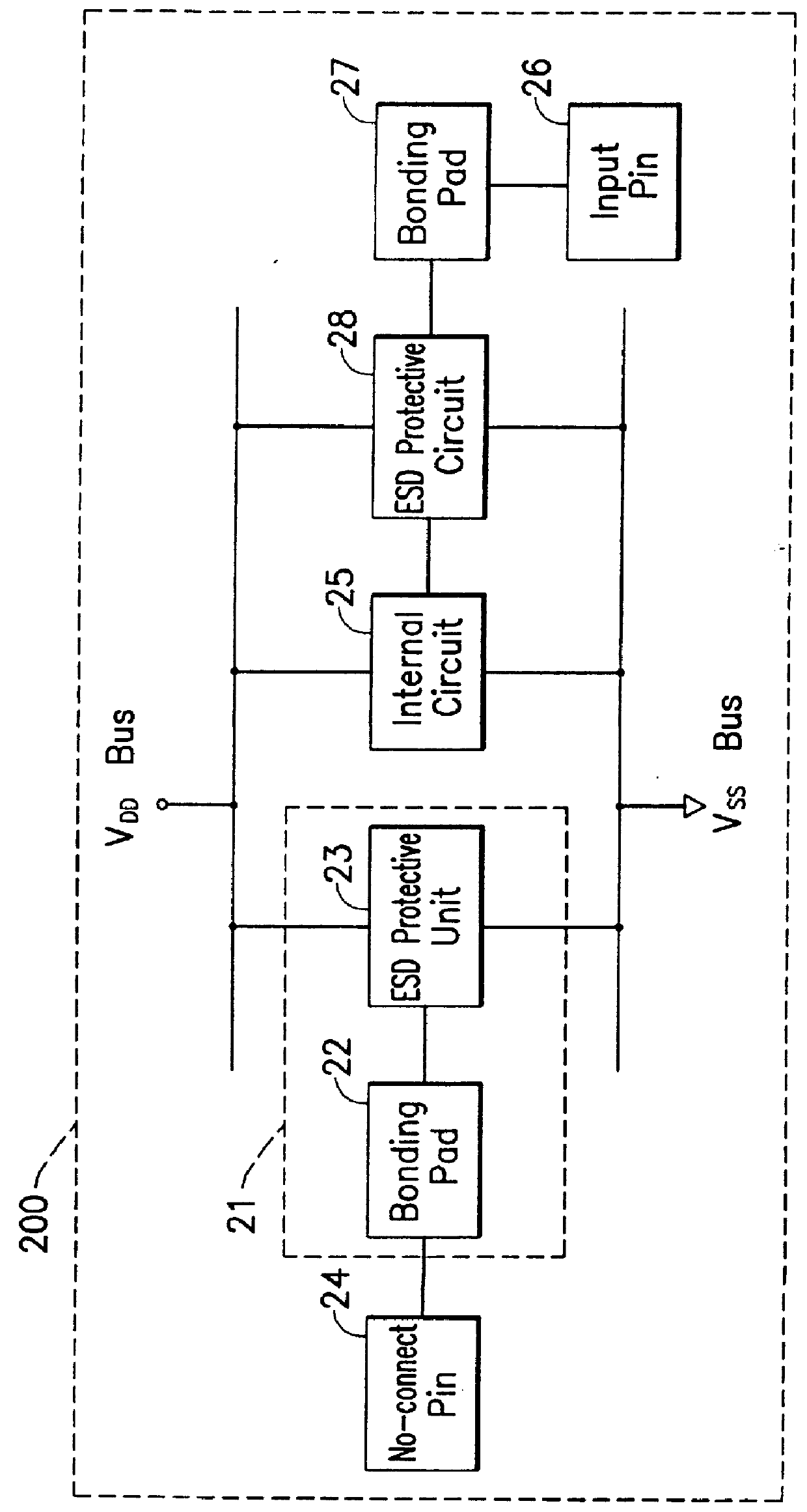
FIG. 2 shows a schematic block diagram of an IC package 200, including an internal circuit 25, at least one no-connect pin 24, and a wired pin 26 connected to a bonding pad 27. A conventional ESD protective circuit 28 is coupled between the internal circuit 25 and the bonding pad 27 corresponding to the wired pin 26, to provide ESD protection with regard to the internal circuit 25.

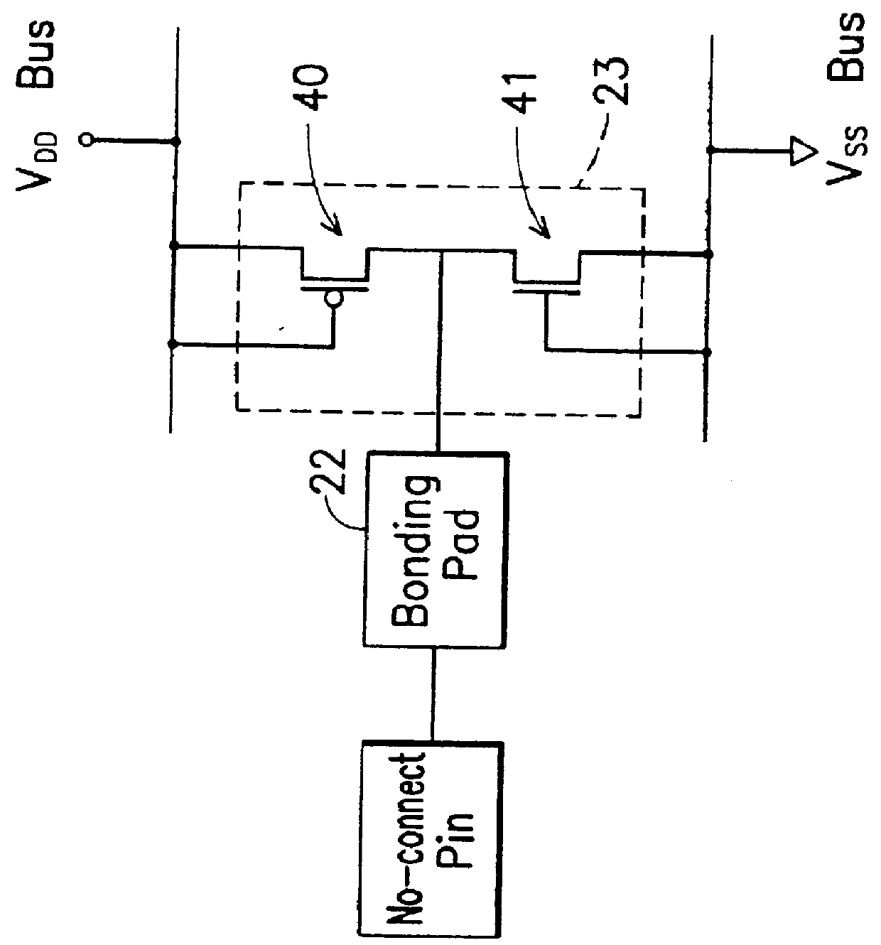
In accordance with the invention, the no-connect pin 24 is coupled to an ESD protective device 21 which is indicated by a dashed outline box. The ESD protective device 21 includes a bonding pad 22 and an ESD protective unit 23. The bonding pad 22 is connected between the no-connect pin 24 and the ESD protective unit 23, while the ESD protective unit 23 is further coupled to the V.sub.DD power bus and the V.sub.SS power bus but not directly connected to the internal circuit 25.

When the no-connect pin 24 receives an ESD stress, the ESD current will flow to the bonding pad 22, and will be subsequently diverte...


PUM


Abstract

An ESD protective device for protection of an integrated circuit (IC) package from electrostatic discharge damage. The ESD protective device protects the internal circuit of the IC connected to wired pins of the IC package against ESD damage due to ESD stress in neighboring no-connect pins. The ESD protective device includes an ESD protective unit coupled to the power bus and a bonding pad coupled between this ESD protective device and the no-connect pin. The ESD protective unit causes ESD stress applied to the no-connect pin to be diverted to the power bus, thus preventing ESD transfer between a no-connect pin and an active pin, which could damage the internal circuit.

Description

1. Field of the InventionThe invention relates to electrostatic discharge (ESD) protection in integrated circuit (IC) packages, and more particularly, to ESD protective devices provided to selected no-connect pins on an IC package for protection of the IC package and internal circuit against ESD stress applied to the no-connect pins.2. Description of Related ArtElectrostatic discharge (ESD) is a movement of static electricity from a nonconductive surface, which could cause damage to semiconductors and other circuit components in ICs. A person walking on a carpet, for instance, can carry an amount of electrostatic charge up to several thousands of volts under high humidity conditions and over 10,000 volts under low humidity conditions. When touching ICs by hand, the instantaneous power levef of the ESD could cause severe damage to the ICs. CMOS (complementary metal-oxide semiconductor) logic ICs are especially vulnerable to ESD.To protect IC packages against ESD damage, various solut...

Claims


Application Information

Patent Timeline
IPC IPC(8): H01L23/60H01L23/48H01L23/58H01L23/50
CPCH01L23/50H01L23/60H01L2224/48247H01L2224/49171H01L2924/13091H01L24/49H01L24/48H01L2924/13034H01L2924/00H01L2924/00014H01L2224/05554H01L2924/14H01L2224/45099H01L2224/05599H01L2224/85399H01L2224/45015H01L2924/207
Inventor LIN, SHI-TRON
Owner WINBOND ELECTRONICS CORP
Why Eureka
Try Eureka