Thin film transistor array panel and manufacturing method thereof

a technology of thin film transistors and array panels, which is applied in the direction of instruments, semiconductor devices, optics, etc., can solve the problems of esd damage between layers, severe, and melts of silicon layers, and achieve the effect of preventing esd damag

Active Publication Date: 2006-03-02
SAMSUNG DISPLAY CO LTD
View PDF7 Cites 3 Cited by
  • Summary
  • Abstract
  • Description
  • Claims
  • Application Information

AI Technical Summary

Benefits of technology

[0011] A motivation of the present invention is to provide a TFT array panel and a manufacturing method thereof for preventing ESD damage due to impurity implantation.

Problems solved by technology

The ESD damages are generated between adjacent gate members and they become severe when the sizes of the gate members are different since the voltage difference become larger.
The large current due to the ESD makes damage on a gate insulating layer located between the gate lines and the silicon active layers and it melts the silicon layers to be agglomerated or evaporated.
However, since the protection diodes are activated after forming the data lines, there is no ESD protection mechanism before the formation of the data lines.
Although a technique for minimizing the difference in the areas between adjacent gate members is suggested, there is difficulty in designing the gate members to fixed areas.
In addition, this technique is somewhat effective in reducing defect ratio, but it is insufficient for preventing the ESD damage due the difference in impurity doping amount between the gate members.

Method used


Image

  • Thin film transistor array panel and manufacturing method thereof
  • Thin film transistor array panel and manufacturing method thereof
  • Thin film transistor array panel and manufacturing method thereof

Examples


Embodiment Construction

[0032] The present invention now will be described more fully hereinafter with reference to the accompanying drawings, in which preferred embodiments of the inventions are shown.

[0033] In the drawings, the thickness of layers and regions are exaggerated for clarity. Like numerals refer to like elements throughout. It will be understood that when an element such as a layer, region or substrate is referred to as being “on” another element, it can be directly on the other element or intervening elements may also be present. In contrast, when an element is referred to as being “directly on” another element, there are no intervening elements present.

[0034] Now, polysilicon TFT array panels and manufacturing methods thereof according to an embodiment of the present invention will be described in detail with reference to the accompanying drawings.

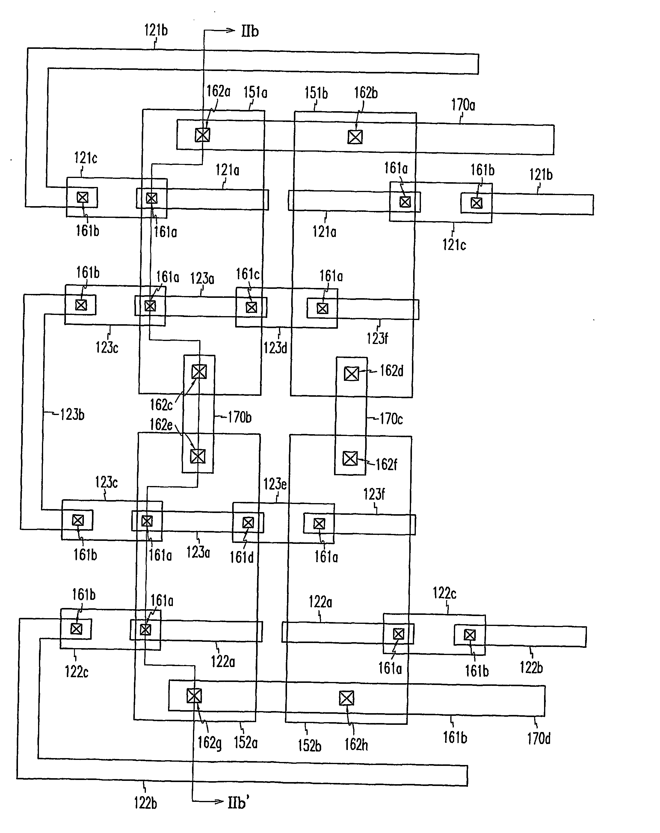
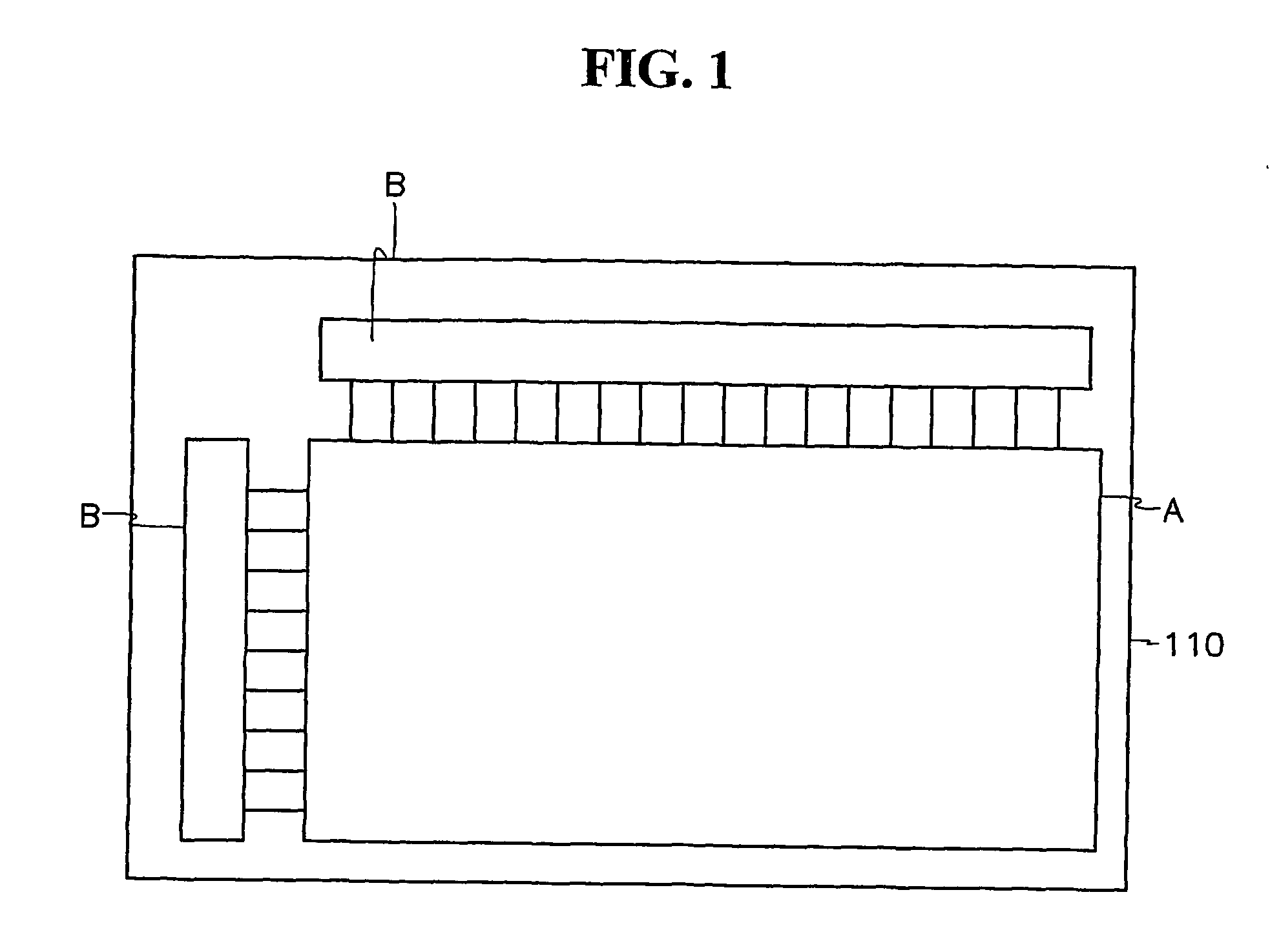
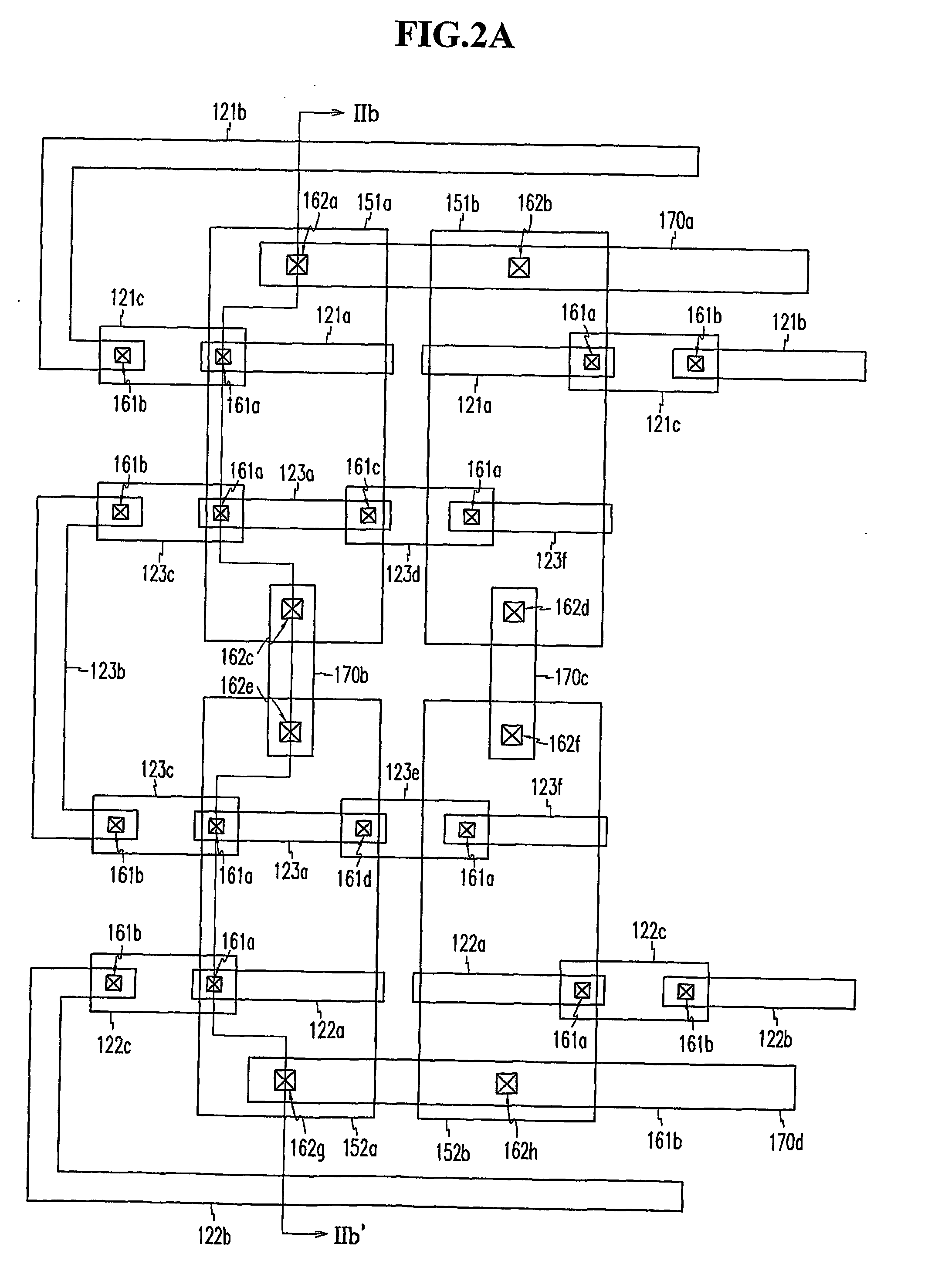
[0035]FIG. 1 is a schematic diagram of a TFT array panel according to an embodiment of the present invention.

[0036] Referring to FIG. 1, a TF...


PUM

PropertyMeasurementUnit
conductivityaaaaaaaaaa
semiconductoraaaaaaaaaa
gate-off voltageaaaaaaaaaa

Abstract

A thin film transistor array panel includes: an insulating substrate (110); first and second semiconductor members (151 a,b) formed on the substrate and having opposite conductivity; a first gate member (121a) insulated from the first and the second semiconductor members and overlapping one of the first and the second semiconductor members; a second gate member (122a) formed on the same layer as the first gate member (121a), separated from the first gate member, and insulated from the first and the second semiconductor members (151 a,b), the second gate member (122a) not overlapping the first and the second semiconductor members; a first data member (162) connected to one of the first and the second semiconductor members (151 a,b) and insulated from the first (121a) and the second (122a) gate members; and a first connection (123) formed on the same layer as the first data member and connecting the first gate member (121a) and the second gate member (122a).

Description

BACKGROUND OF THE INVENTION [0001] (a) Field of the Invention [0002] The present invention relates to a thin film transistor array panel and a method thereof, and in particular, to a polysilicon thin film transistor array panel. [0003] (b) Description of the Related Art [0004] Thin film transistors (TFT) are used for driving pixels in a liquid crystal display (LCD) and electro luminescence (EL) display. A panel including the TFTs also includes a plurality of gate lines transmitting scanning signals for turning on and off the TFTs and a plurality of data lines transmitting data signals for the display of the pixels. [0005] The TFTs include polysilicon or amorphous silicon as active layers. When the display panel includes polysilicon TFTs for switching the data signals to be supplied to the pixels, driving circuits for generating the scanning signals and the data signals can be also formed on the display panel along with the TFTs for the pixels such that cost and complexity for mounti...

Claims


Application Information

Patent Timeline
Patent Type & Authority Applications(United States)
IPC IPC(8): G02F1/1333H01L21/77H01L21/84G02F1/136H01L27/12
CPCH01L27/124G02F1/136
Inventor HWANG, CHANG-WONCHUNG, WOO-SUK
Owner SAMSUNG DISPLAY CO LTD
Why Eureka
Try Eureka