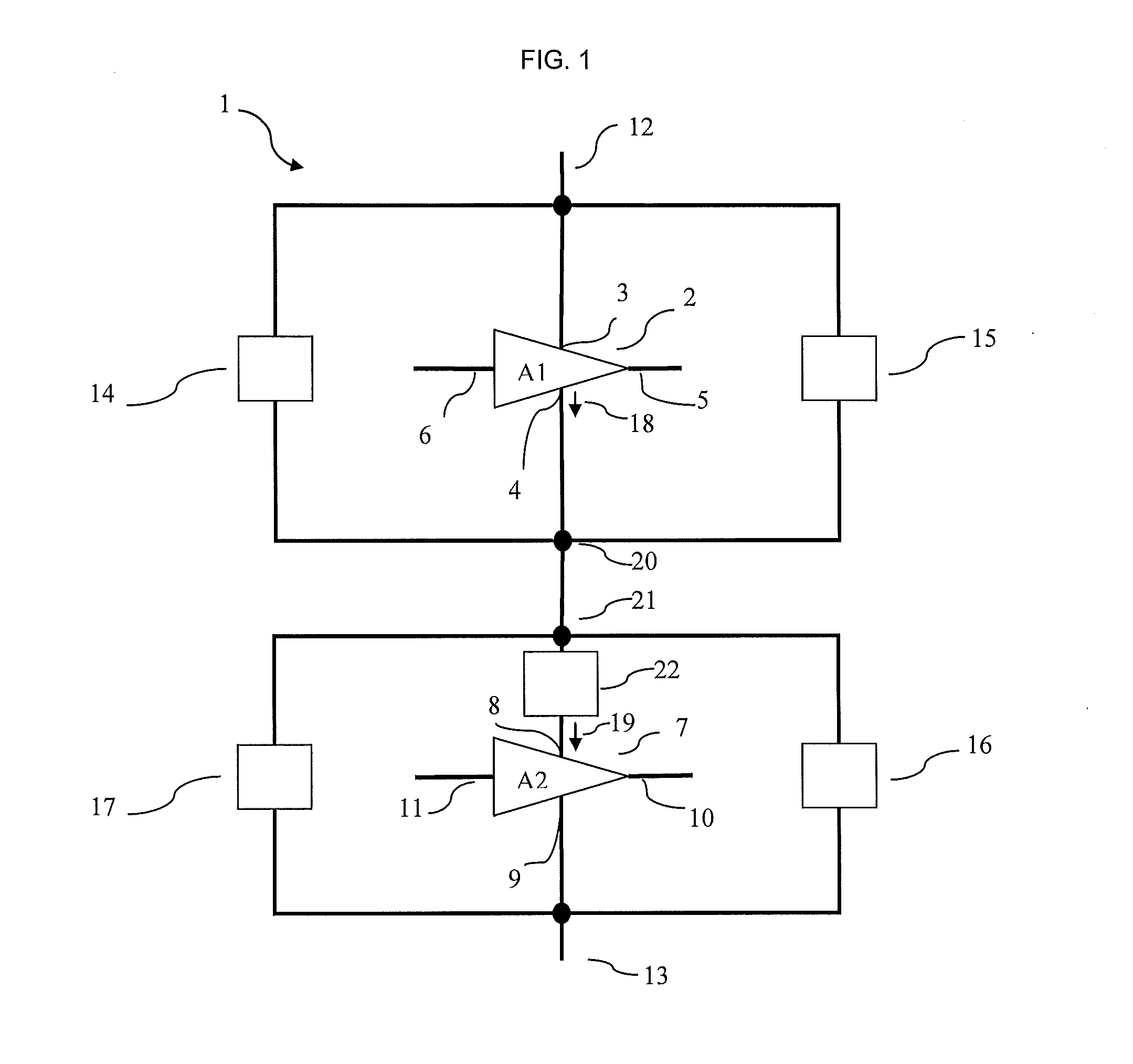
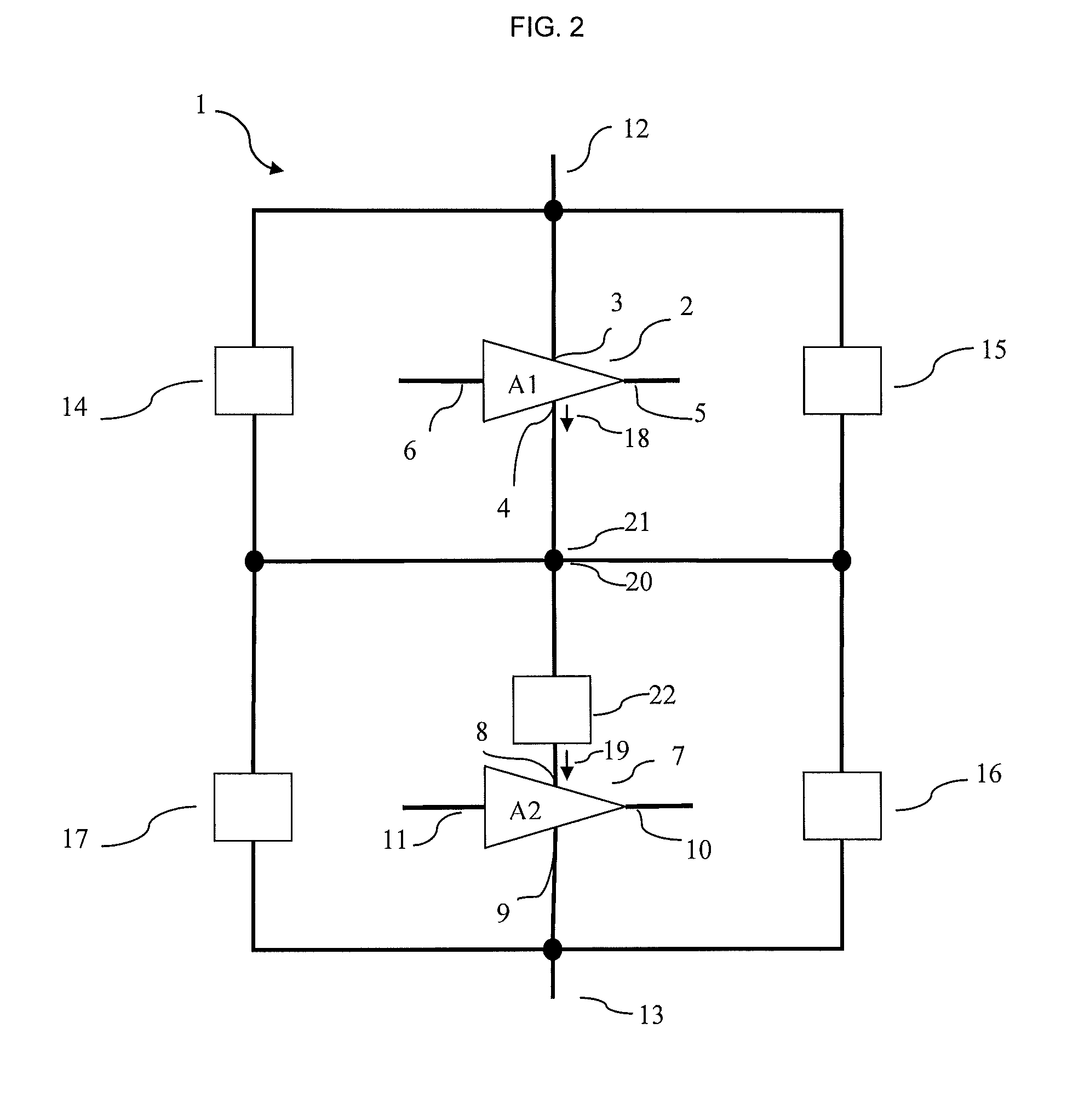
Low power integrated circuit

a low-power, integrated circuit technology, applied in the direction of amplifiers, amplifiers with min 3 electrodes or 2 pn junctions, amplifiers, etc., can solve the problems of increasing the requirement of electronic components, the challenge of wire-based interconnect devices, and the difficulty of wire-based interconnects of the future, so as to improve the noise figure, increase the current consumption, and improve the effect of nois

Active Publication Date: 2010-08-26
MELLANOX TECH DENMARK APS
View PDF11 Cites 6 Cited by
  • Summary
  • Abstract
  • Description
  • Claims
  • Application Information

AI Technical Summary

Benefits of technology

[0036]In one embodiment the voltage stabilizer comprises an inductive load. In one embodiment the voltage stabilizer comprises one or more active components such as a Zener diode or operational amplifiers. An example of such a voltage stabilizer is a Zener diode connected in parallel with the second amplifier. In this way the diode may ensure that a specific voltage is maintain across the second amplifier and conduct excess current if required. Obviously, there are an extensive number of possible designs with a similar or equivalent functionality such as applying an active diode circuit instead of a Zener diode. In one embodiment the voltage stabilizer feedback loop is arranged so that the voltage is stabilized relative to a voltage reference.
[0037]In one embodiment the first and / or second amplifier comprises a series of two or more cascaded amplifiers. These cascaded amplifiers are connected in series along the signal path whereas the supply ports of the cascaded amplifiers are connected in parallel. In one embodiment all amplifiers have a substantially equal amplification factor and in one embodiment the amplification of two or more amplifiers of the set is different. In one embodiment the amplifiers of the set have an increasing amplification factor along the signal path in the direction from input to output of the integrated circuit. In one embodiment cascading provides an improved noise figure relative to a single amplifier. In one embodiment cascading of one amplifier allows the designer to tune the current consumption of that amplifier e.g. to match the current consumption to that of the other amplifier.
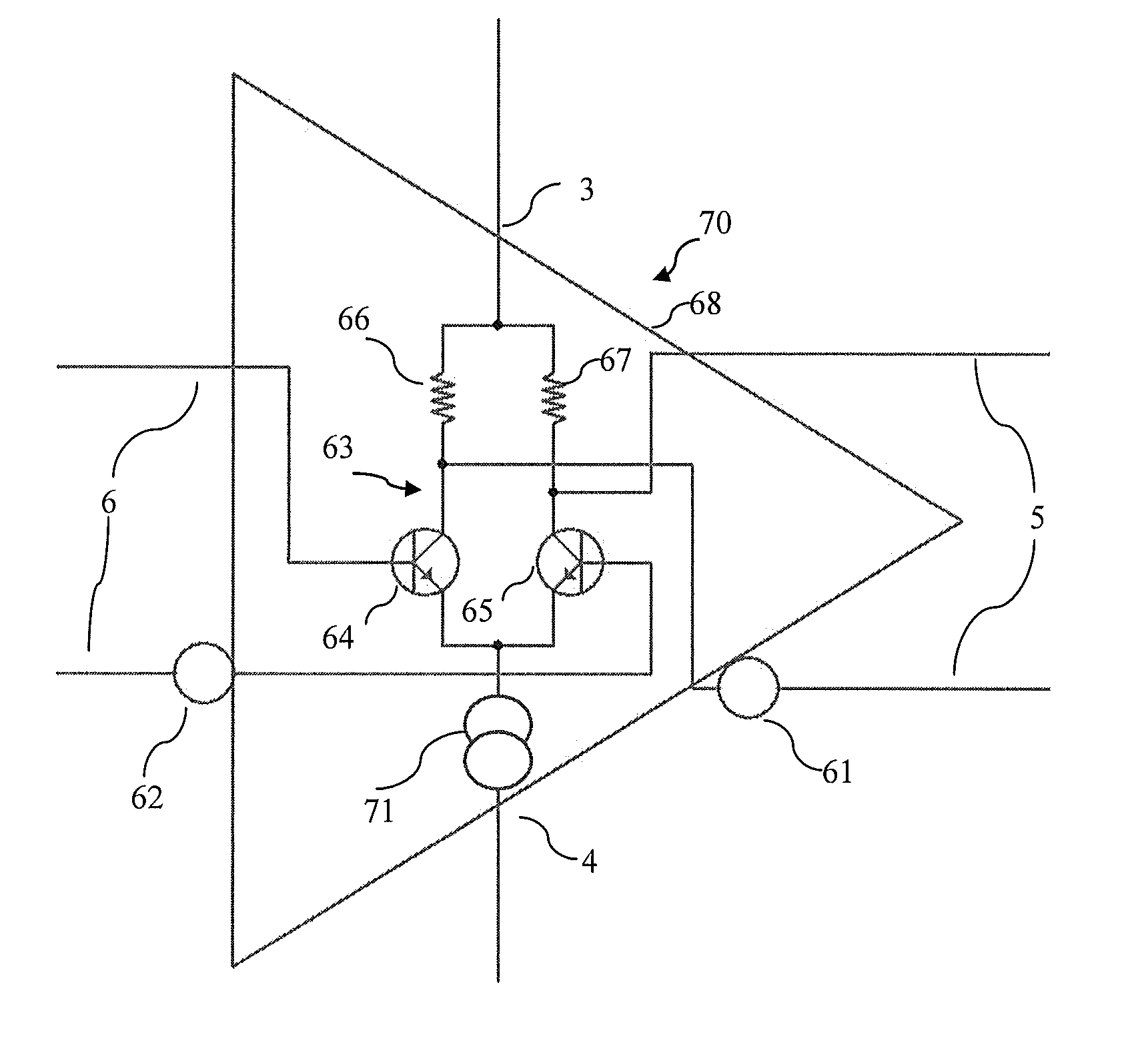
[0038]In one embodiment the first amplifier is arranged to have a higher current consumption than the second amplifier i.e. a higher current exiting from the output supply port of the first amplifier than entering the input supply port of the second amplifier the difference referred to as excess current. In one embodiment the integrated circuit comprises a drain path arranged to pass at least part of the excess current around the second amplifier. In one embodiment the second amplifier is arranged to have a higher current consumption than the first amplifier i.e. a higher current entering the input supply port of the second amplifier than exiting the output supply port of the second amplifier the difference referred to as added current. In one embodiment the integrated circuit comprises an added current path arranged to pass at least part of the added current to the second amplifier. In one embodiment the added path comprises a current source.
[0039]In one embodiment the integrated circuit is arranged to comprise a regulator circuit arranged to adjust the current into the input supply port of the second amplifier. In one embodiment said regulator is a programmable circuit so that the current added or subtracted may be set by programming. In one embodiment the said regulator regulates relative to a reference, such as a current and / or a voltage reference. In one embodiment said regulator functions as a voltage stabilizer such as discussed above.
[0040]In one embodiment the inherent current consumption of the first amplifier in use is substantially matched to the inherent current consumption of the second amplifier in use.
[0041]In one embodiment the integrated circuit comprises N amplifiers, where N is an integer larger than 1, each amplifier comprising an input signal port, an output signal port, an input supply port and an output supply port wherein the supply ports of said amplifiers are connected in series via a supply connection wherein said integrated circuit is arranged so that two or more of the amplifiers are decoupled in a similar manner to first and second amplifiers. In this way the invention is not limited to the first and second amplifiers sharing supply current but may comprise three or more amplifiers sharing supply current. In one embodiment one or more of said N amplifiers are formed by a set of cascaded amplifiers.

Problems solved by technology

It is apparent that wire-based interconnect devices will be challenged to enabling even higher operating frequencies.
However, besides challenges with regard to bandwidth, the wire-based interconnects of the future may struggle significantly with a high power consumption.
The power requirement of electronic components typically increases with increased bandwidth, which in some cases results in increased cooling requirement which further increases power consumption of the electronic system.
The power and cooling requirement may be particularly challenging to meet in data centers where larger quantities of servers are pooled and closely spaced.
Such pooling inherently requires large quantities of interconnects which therefore may add significantly to the power and cooling requirements of the datacenter.
A substantial amplification of the incoming signal is often required so that a substantial amount of power is required by the receiver.
Such circuits are likely not suitable for high speed binary communication and other types of communication which require a wide band of frequencies.
Coils are often not available to the integrated circuit designer and to achieve sufficient decoupling to obtain decoupling for a large frequency span a capacitor will have to be very large which would be prohibitive to a compact integrated design.
Furthermore such as a capacitor, or an equivalent formed by active components, may introduce a significant amount of noise.
This is sometimes the case when only a single power supply voltage is available and one or more components require a relatively high voltage.
Other constraints may impose the use of a relatively high voltage such as system- or communications standards.
However, in one embodiment such spikes consist primarily of frequency components which experience relatively high loss when travelling along the conductors providing positive, negative, or ground potentials which may form a link between the integrated circuit and said other components.
The challenge for such a device may be to achieve sufficient decoupling over the required bandwidth.
Such imperfections may be one or more of inductive coupling, bandwidth limitations and parasitic capacitances.
However, in an integrated design space may not be available or may be related to a high cost due to the required chip area.

Method used


Image

  • Low power integrated circuit
  • Low power integrated circuit
  • Low power integrated circuit

Examples


Embodiment Construction

[0055]In FIG. 1 the first amplifier 2 has a signal input 6, a signal output 5, an input supply port 3 and an output supply port 4. Similarly the second amplifier 7 has a signal input 11, a signal output 10, an input supply port 8 and an output supply port 9. The supply ports of the amplifiers are arranged to be supplied from the positive supply 12 and the negative supply 13. In the current example, as well as this text as a whole, positive and negative supply need not necessarily be supplies as such but in principle indicates a difference in potential in the positive supply relative to the negative supply suitable for supplying the necessary current and / or headroom to the circuit, often preferably sufficiently constant to provide a substantial constant performance of the first and second amplifiers. Accordingly, in one embodiment the circuit is implemented between a positive supply and ground. In one embodiment the circuit is implemented with additional circuitry above the indicated...


PUM


Abstract

The present invention relates to an integrated electrical circuit in particular a receiver or driver suitable for broadband communication, such as optical interconnect. The circuit comprises two amplifiers which share current supply wherein the integrated circuit is arranged so that cross talk via this current supply is avoided over a large range of frequencies.

Description

TECHNICAL FIELD[0001]The invention relates to the field of integrated circuitry wherein the integrated circuit comprises at least one first amplifier and at least one second amplifier each comprising an input signal port, an output signal port, an input supply port and an output supply port. The invention in particular relates to an integrated circuitry for optical communication in particular for optical interconnects such as integrated driver and receiver circuitry.BACKGROUND ART[0002]The demands for ever-increasing bandwidths in digital data communication equipment at reduced power consumption levels are constantly growing. These demands not only require more efficient integrated-circuit components, but also higher performance interconnects and devices. Indeed, as one example, the International Technology Roadmap for Semiconductors (ITRS) projects that high performance chips in the very near future will have operating frequencies, both on-chip and off-chip, rising above 50 GHz. Co...

Claims


Application Information

Patent Timeline
Patent Type & Authority Applications(United States)
IPC IPC(8): H03F3/45H03F1/00
CPCH03F1/26H03F3/08H03F3/45085H03F2203/45702H03F2200/36H03F2200/405H03F2203/45138H03F3/45475H03F1/0283
Inventor CHRISTENSEN, KENN
Owner MELLANOX TECH DENMARK APS
Why Eureka
Try Eureka