Semiconductor device

Active Publication Date: 2007-02-01
PANASONIC CORP
View PDF6 Cites 29 Cited by
  • Summary
  • Abstract
  • Description
  • Claims
  • Application Information

AI Technical Summary

Benefits of technology

[0020] In this case, the diode pair is preferably plural in number. Thus, the surge resistance can be further improved.
[0021] In the semiconductor device of this invention, the substrate preferably has a conducting property, and the semiconductor device preferably further includes a first via plug for electrically connecting the source electrode and the substrate to each other; and a second via plug for electrically connecting a diode connected to the gate electrode out of the plural diodes and the ohmic electrode of another diode disposed in an opposite end to each other. Alternatively, the substrate preferably has a cond

Problems solved by technology

Furthermore, since the diode can be formed by forming a third nitride semiconductor layer and an ohmic electrode on t

Method used


Image

  • Semiconductor device
  • Semiconductor device
  • Semiconductor device

Examples


embodiment 1

Modification of Embodiment 1

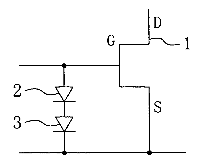
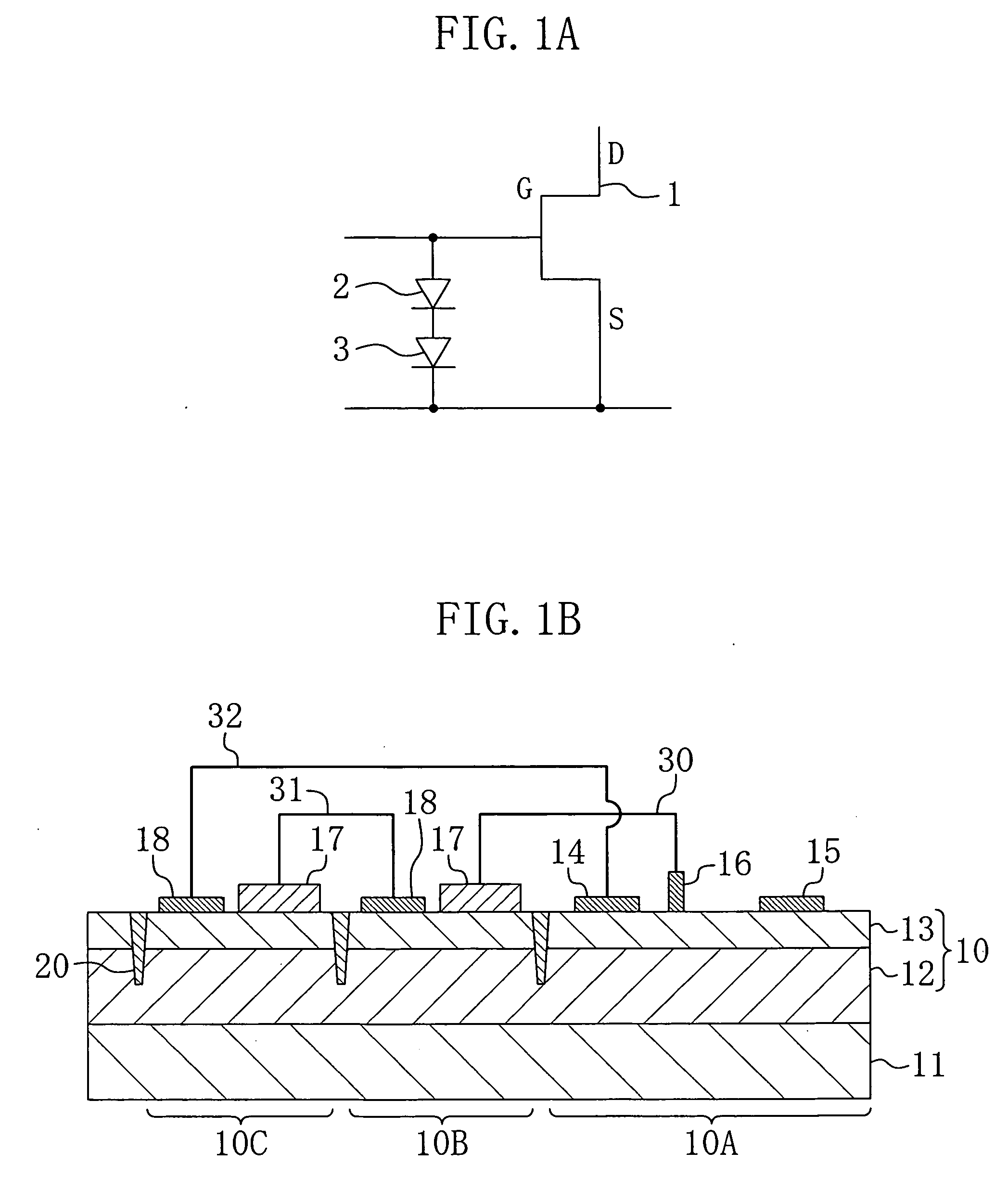
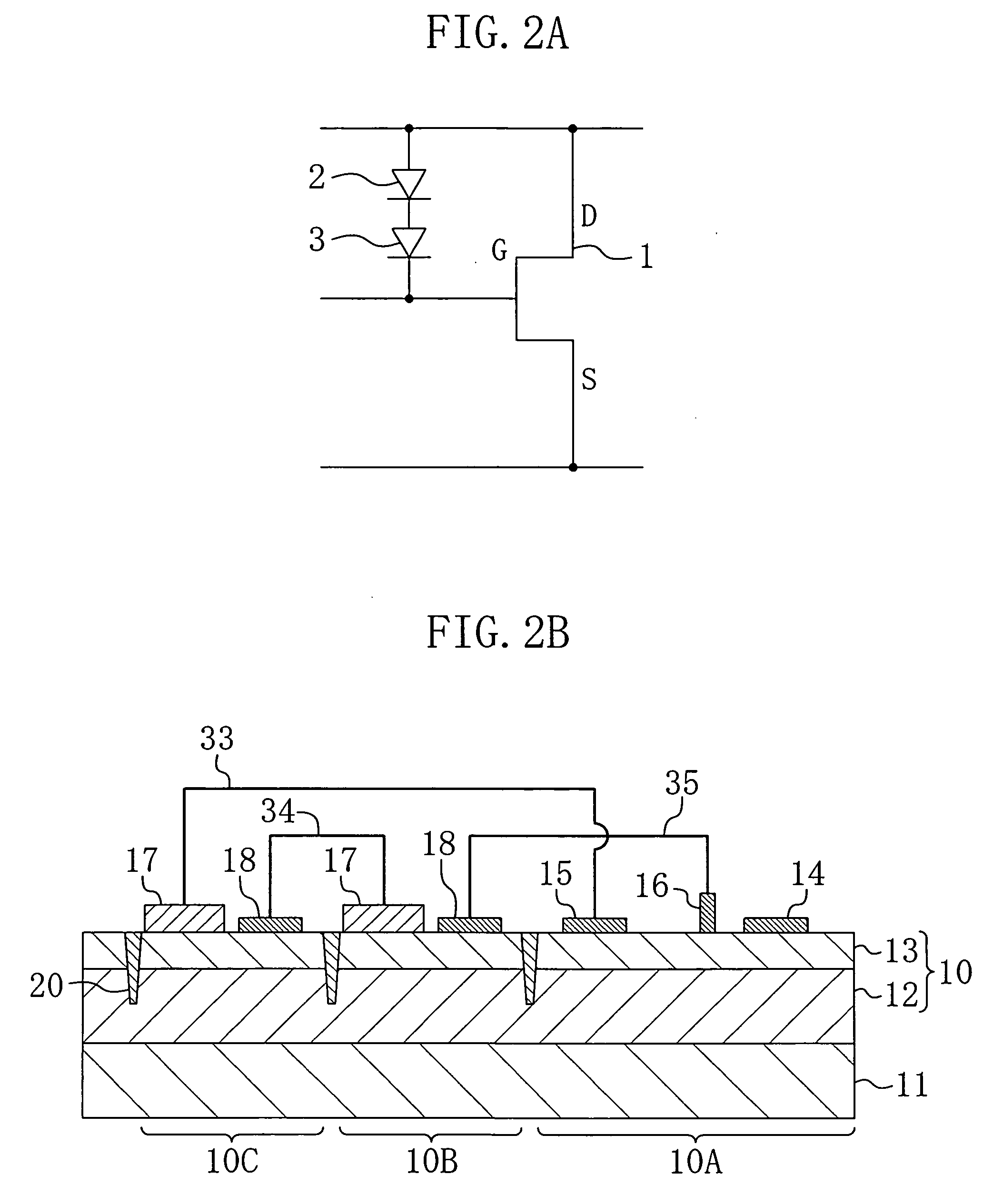
[0040] Now, a modification of Embodiment 1 of the invention will be described with reference to the accompanying drawings. FIGS. 2A and 2B show a semiconductor device according to the modification of Embodiment 1, and specifically, FIG. 2A is an equivalent circuit diagram thereof and FIG. 2B is a cross-sectional view thereof. In FIGS. 2A and 2B, like reference numerals are used to refer to like elements shown in FIGS. 1A and 1B so as to omit the description.

[0041] As shown in FIGS. 2A and 2B, protection diodes are connected between a gate and a drain in the semiconductor device of this modification. A drain electrode 15 of an HFET 1 and a third semiconductor layer 17 corresponding to an anode of a first pn junction diode 2 are connected to each other through an interconnection 33. An ohmic electrode 18 corresponding to a cathode of the first pn junction diode 2 and the third semiconductor layer 17 corresponding to an anode of a second pn junction diode 3...

embodiment 2

Modification of Embodiment 2

[0055] Now, a modification of Embodiment 2 of the invention will be described with reference to the accompanying drawing. FIG. 6 shows the cross-sectional structure of a semiconductor device according to the modification of Embodiment 2. In FIG. 6, like reference numerals are used to refer to like elements shown in FIGS. 3A and 3B.

[0056] The equivalent circuit of the semiconductor device of this modification is the same as that of the semiconductor device of Embodiment 2, and specifically, two diodes working as protection elements are connected between the gate and the source of an HFET in a back to back manner. As shown in FIG. 6, the semiconductor device of this modification is formed on a conducting substrate 41, and a via plug 42 for electrically connecting a source electrode 14 of the HFET and the substrate 41 to each other and a via plug 43 for electrically connecting an ohmic electrode 19 of a second pn junction diode 3 and the substrate 41 to eac...


PUM


Abstract

A semiconductor device includes a field effect transistor and a pn junction diode formed on a substrate. The field effect transistor has a source electrode, a drain electrode and a gate electrode formed on an element forming layer including a plurality of nitride semiconductor layers. The diode includes a p-type nitride semiconductor layer selectively formed on the element forming layer and an ohmic electrode, and has a pn junction formed between an n-type region of a two-dimensional electron gas generated on a heterojunction interface and a p-type region of the p-type nitride semiconductor layer. The diode is electrically connected to the gate electrode and forms a current path for allowing an excessive current caused in the gate electrode to pass.

Description

CROSS-REFERENCE TO RELATED APPLICATIONS [0001] This application claims priority under 35 U.S.C. §119 on Patent Application No. 2005-219286 filed in Japan on Jul. 28, 2005, the entire contents of which are hereby incorporated by reference. The entire contents of Patent Application No. 2006-190019 filed in Japan on Jul. 11, 2006 are also incorporated by reference. BACKGROUND OF THE INVENTION [0002] The present invention relates to a semiconductor device, and more particularly, it relates to a semiconductor device including a field effect transistor using a nitride semiconductor and having a protection diode. [0003] A group III-V nitride semiconductor is a compound semiconductor including aluminum (Al), boron (B), gallium (Ga) or indium (In) and nitrogen (N) and represented by a general formula, BwAlxGayInzN (wherein w+x+y+z=1; and 0≦w, x, y, z≦1). [0004] A nitride semiconductor has various advantages such as a large band gap and a resultant high breakdown voltage, high electron satura...

Claims


Application Information

Patent Timeline
IPC IPC(8): H01L29/74
CPCH01L29/2003H01L27/0255H01L27/0605H01L27/0629
Inventor HIROSE, YUTAKATANAKA, TSUYOSHI
Owner PANASONIC CORP
Why Eureka
Try Eureka