Digital-to-analog conversion with an interleaved, pulse-width modulated signal

a digital-to-analog conversion and pulse-width modulation technology, applied in the direction of electronic circuit testing, transmission systems, hinges, etc., can solve the problem of common problems such as the conversion of digital signals to analog signals, and achieve the effect of increasing the number of logic state changes within the pattern repetition time, maximizing the number of logic state changes given predetermined subdivision into time subblocks, and increasing the accentuation of higher-frequency frequency components

Inactive Publication Date: 2005-09-22
PATENT TREUHAND GESELLSCHAFT FUR ELECTRIC GLUEHLAMPEN MBH
View PDF8 Cites 6 Cited by
  • Summary
  • Abstract
  • Description
  • Claims
  • Application Information

AI Technical Summary

Benefits of technology

[0012] The reordering is intended to take place in such a way that the number of logic state changes within the pattern repetition time is increased. Thus, if, for example, a pattern repetition time having precisely one logic positive time block and precisely one logic negative time block is used as the basis, two logic state changes are allotted to this pattern repetition time in the original state. If, however, the time subblocks are redistributed, in many cases more than two logic state changes will occur within the pattern repetition time. In the case which is preferred according to the invention, the number of logic state changes given predetermined subdivision into time subblocks is maximized. Finer subdivision of course allows maximization to an even larger number of state changes.
[0013] Simply reordering the time subblocks given constant logic values for the respective subblocks does not change the average value of the signal, which is obtained as an analog value by means of the low-pass filtering. However, the reordering makes it possible to achieve greater accentuation of higher-frequency frequency components and thus to achieve better filterability of the signal by means of the low-pass filter. If, for illustrative purposes, a low-pass filter in the form of a conventional RC element is envisaged, as a result of the reordering according to the invention of the time subblocks, the time intervals between the state changes are shorter, with the result that charge-reversal processes with smaller voltage amplitudes occur in the filter capacitor. The filtered signal thus has a “ripple” having a smaller amplitude and is thus filtered more effectively. In other words, it is possible to use simpler filters, for example those having smaller capacitors. Another possibility which in this case may come to the fore as a priority in circuit design or else may at the same time be of relevance is the possibility of smaller output impedances and thus smaller shifts as a result of fluctuating output currents.
[0018] A further preferred refinement envisages that for the bit interchange, for example also for bit inversion in accordance with the above explanation, a so-called look-up table is used, i.e. a memory in which the bit interchange is implemented by means of the memory entries at the respective addresses. In this manner, even more complex interchange patterns can be implemented easily if the structure of the look-up table is established. In particular, it would thus also be possible to implement complete even distribution of the time subblocks within the pattern repetition time.

Problems solved by technology

The conversion of digital signals to analog signals is a common problem in various fields of electronics.

Method used


Image

  • Digital-to-analog conversion with an interleaved, pulse-width modulated signal
  • Digital-to-analog conversion with an interleaved, pulse-width modulated signal
  • Digital-to-analog conversion with an interleaved, pulse-width modulated signal

Examples


Embodiment Construction

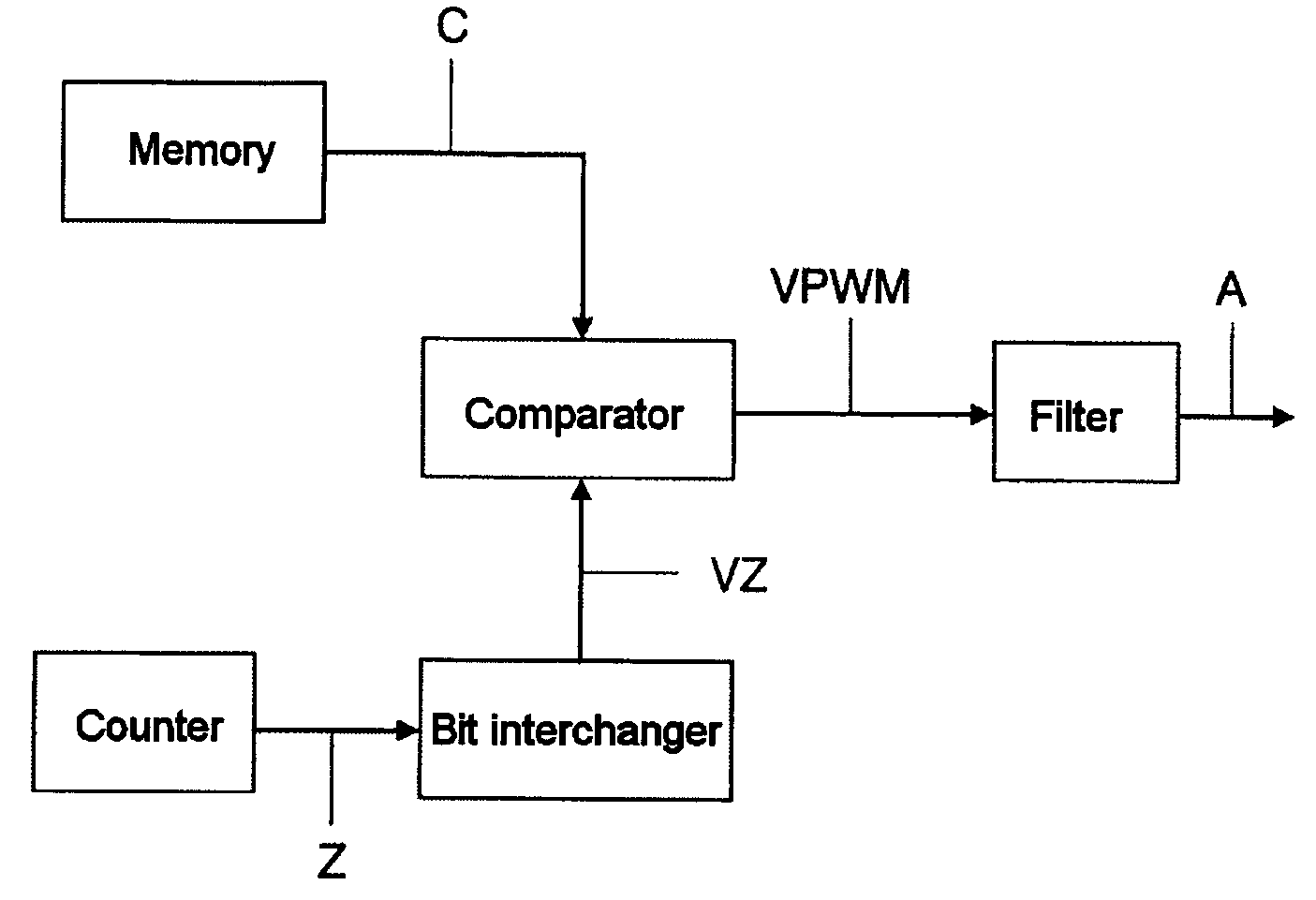
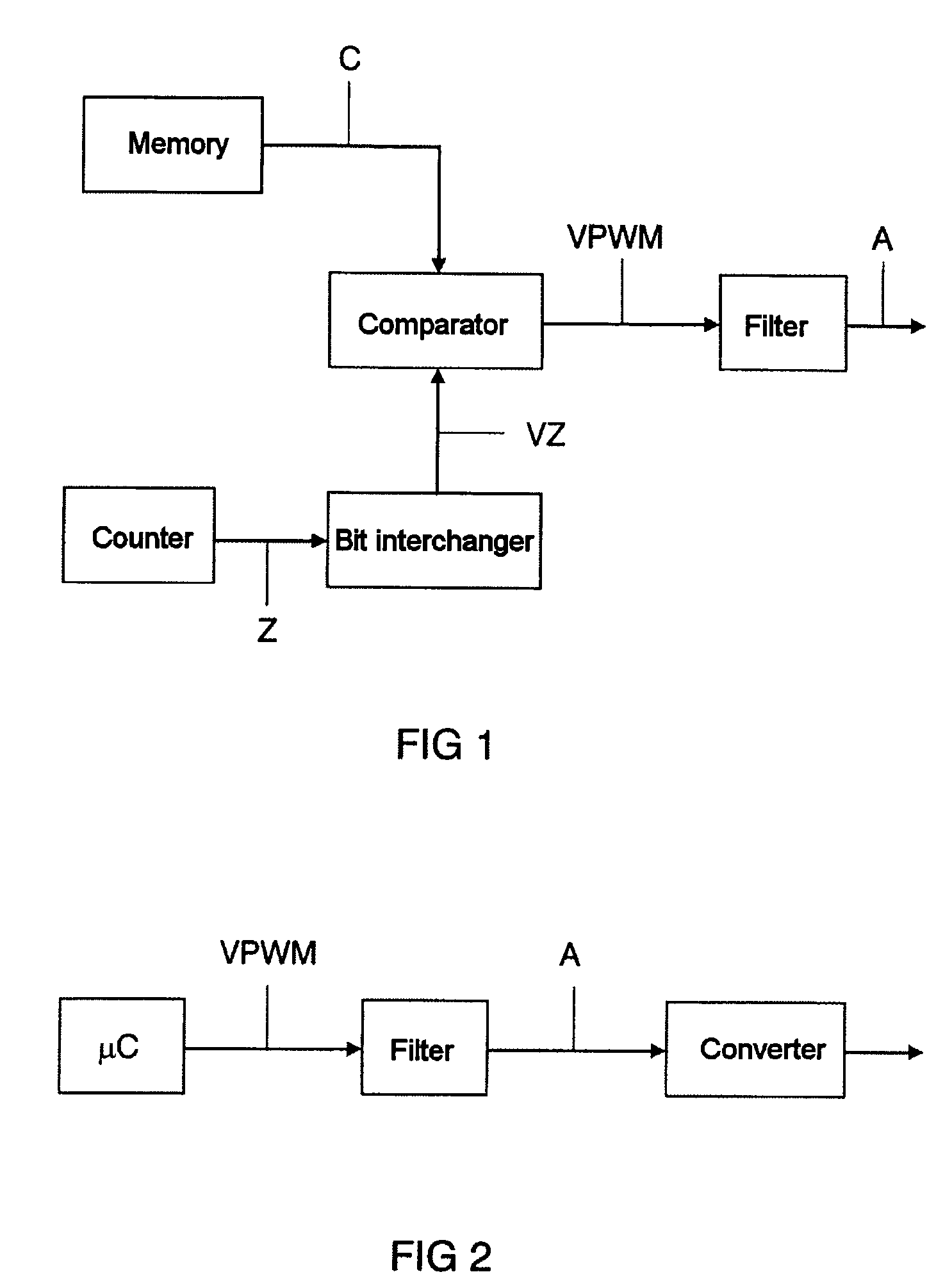
[0032]FIG. 1 shows, using a block diagram, the principle of the invention in a first exemplary embodiment. The method steps explained below with reference to separate components are implemented in this exemplary embodiment actually inside a microcontroller shown in FIG. 2, with the exception of the filter.

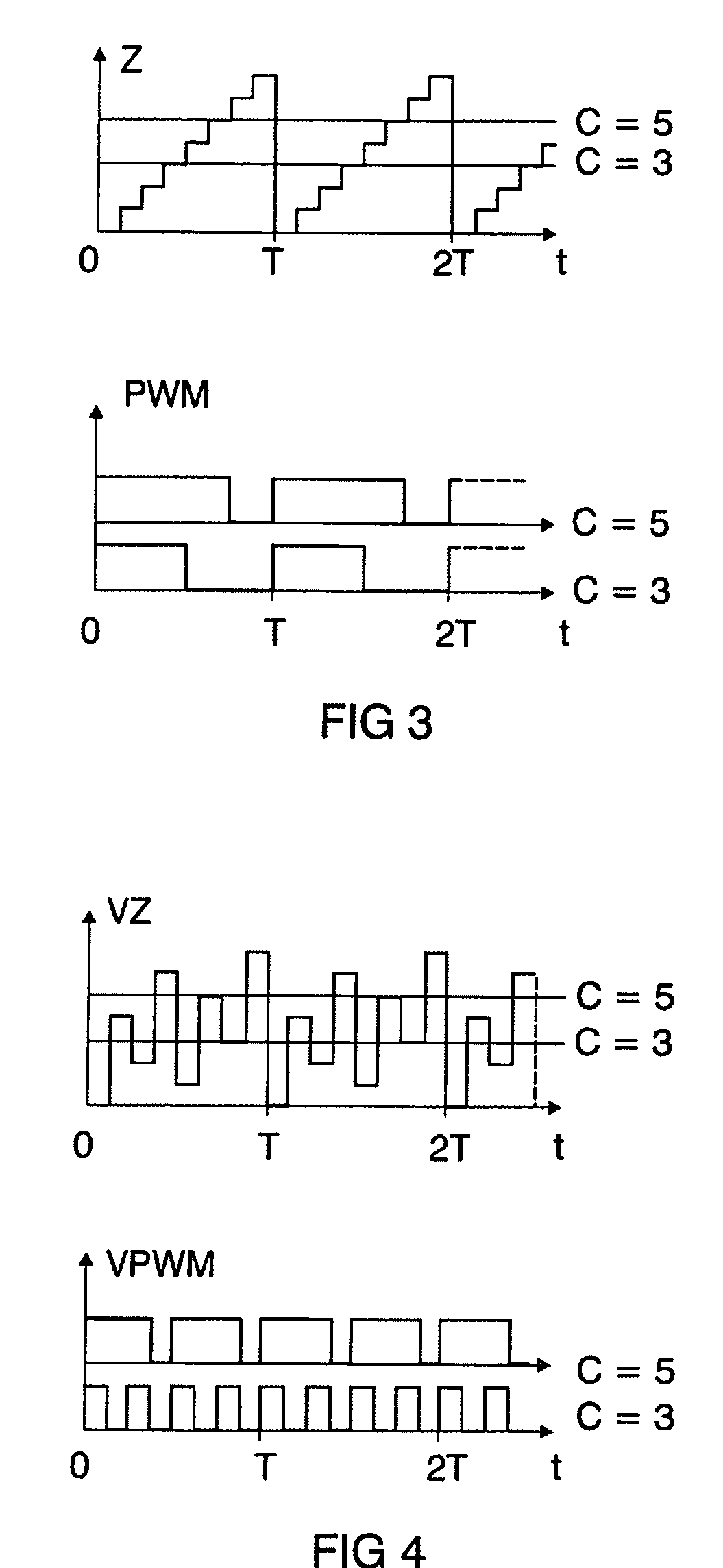
[0033] A memory contains digital values C as the digital signal which are input in a comparator. There, they are compared with a signal which is generated by means of bit interchange from a signal Z from a counter. For this purpose, reference is made to the explanations for FIGS. 3 and 4. The comparator generates, by means of the comparison between the digital signal C and the interleaved counter signal VZ from the bit interchanger, an interleaved, pulse-width modulated signal VPWM which is given to a filter, in this case a second-order RC element, and is filtered there to form an analog signal A.

[0034]FIG. 2 shows, likewise using a block diagram, an exemplary embodiment in which...


PUM


Abstract

The invention relates to a method and a circuit for digital-to-analog conversion, in which an interleaved pulse-width modulation signal (VPWM) is low-pass-filtered.

Description

TECHNICAL FIELD [0001] The present invention relates to a method and a circuit for digital-to-analog conversion. BACKGROUND ART [0002] The conversion of digital signals to analog signals is a common problem in various fields of electronics. In addition to various other methods, low-pass filtering, inter alia, of a pulse-width modulated signal is known. In the case of the pulse-width modulated signal, the duration of a specific logic level, considered on its own or else as a so-called duty ratio in relation to the duration of the other logic level, represents the information to be transmitted. If averaging over time is now carried out by means of low-pass filtering, an analog signal is established by the average value and this signal continuously follows the time duration of the logic level or the duty ratio. DISCLOSURE OF THE INVENTION [0003] The invention is based on the technical problem of specifying a novel method and a novel circuit for digital-to-analog conversion having favor...

Claims


Application Information

Patent Timeline
Patent Type & Authority Applications(United States)
IPC IPC(8): H03K7/08H03M1/82
CPCH03M1/827H03M1/825E05D3/02E05D5/06E05Y2900/132
Inventor SCHALLMOSER, OSKAR
Owner PATENT TREUHAND GESELLSCHAFT FUR ELECTRIC GLUEHLAMPEN MBH
Why Eureka
Try Eureka