Scanning probe microscopy system for mapping nanostructures on a surface of a sample and metrology frame therefore

a scanning probe and nanostructure technology, applied in scanning probe microscopy, measuring devices, instruments, etc., can solve the problems of system itself, limited application of particular circumstances of the technique, and sample thermal expansion, etc., and achieve high-precision sensing

Active Publication Date: 2019-10-22
NEDERLANDSE ORG VOOR TOEGEPAST NATUURWETENSCHAPPELIJK ONDERZOEK TNO
View PDF8 Cites 0 Cited by
  • Summary
  • Abstract
  • Description
  • Claims
  • Application Information

AI Technical Summary

Benefits of technology

[0005]It is an object of the present invention to provide scanning microscopy system wherein the abovementioned disadvantages have been overcome, and which allows for highly accurate sensing on nanometer scale.
[0010]Preferably, and in accordance with some embodiments, the support struts are arranged on the sample support structure such as to support the sample outside the clamping area, e.g. for allowing large samples to be supported (e.g. 300 mm wafers). The support struts may include at least one element of a group comprising: support burls, support knobs, or flexible or rigid support poles. The struts may for example include a flexible material, or may include a rubber or flexible tip. In other embodiments, the ends or tips of the struts may be smooth and rigid to allow lateral slipping of the sample. A combination of these measures is also possible, e.g. flexible poles having smooth rigid tips.
[0013]In other embodiments of the invention, the clamp is a suction clamp for clamping the sample by means of suction. The use of a suction clamp, for example in combination with a robotic arm type external positioner provides a convenient implementation of the invention that allows placement and replacement of the sample on the clamp in a fast and non-destructive manner. Moreover, suction force can be accurately controlled by controlling the pressure within the clamp during clamping. This allows to control the lateral stiffness provided by the clamp such as to ensure that it is larger than, for example, the lateral stiffness of supporting the sample by the support struts of the support structure, as described above.

Problems solved by technology

Although the above works well for many applications, it does provide some drawbacks that limit application of the technique in particular circumstances.
For example, one of these drawbacks relates to thermal expansion of components, which puts constraints on the achievable accuracy.
However, not only the system itself, but also the sample is subject to thermal expansion.
This particularly becomes problematic for larger samples, e.g. 300 mm wafers.
As may be appreciated, if structures on the surface of the sample are to be mapped on nanometer scale, even the smallest temperature variation may result in an unacceptable inaccuracy in the measurement.

Method used


Image

  • Scanning probe microscopy system for mapping nanostructures on a surface of a sample and metrology frame therefore
  • Scanning probe microscopy system for mapping nanostructures on a surface of a sample and metrology frame therefore
  • Scanning probe microscopy system for mapping nanostructures on a surface of a sample and metrology frame therefore

Examples


Embodiment Construction

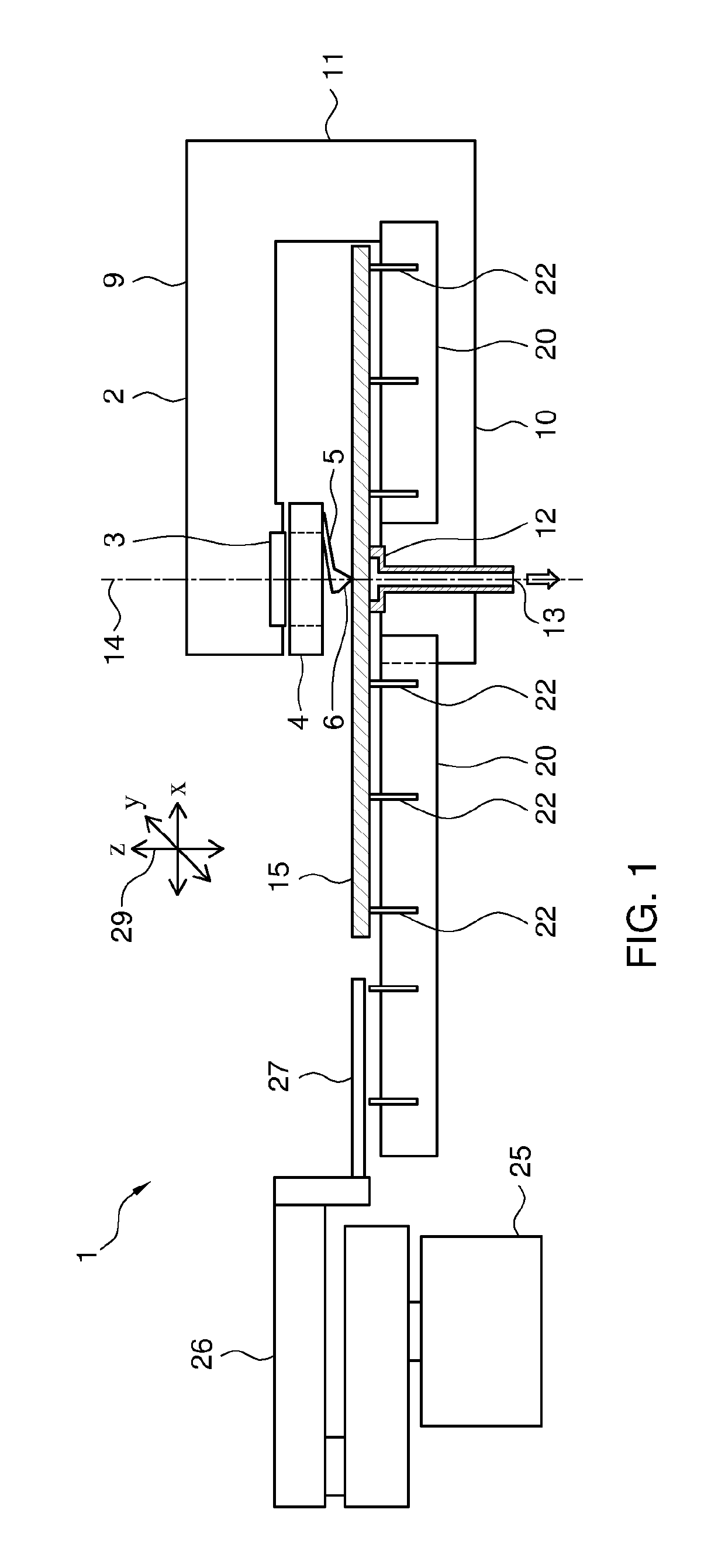
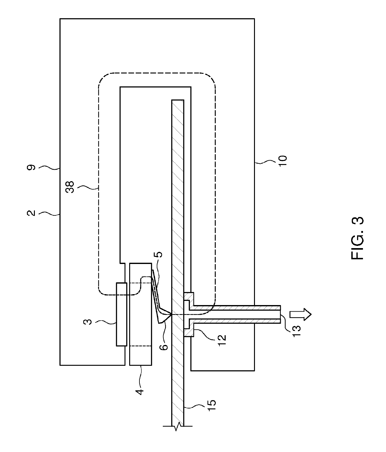
[0020]A system in accordance with the present invention is schematically illustrated in a cross sectional side view in FIG. 1. The scanning probe microscopy system 1 comprises a metrology frame 2 comprising, as illustrated, at least an upper arm 9 and lower arm 10. The upper arm 9 comprises a sensor head 4 mounted on an actuator 3. The actuator 3 enables scanning of the probe 5 of the sensor head 4 across the surface of a sample 15. For example, with reference to the coordinate system 29 schematically illustrated in FIG. 1, the actuator may allow scanning of the probe 5 of the sensor head 4 in the x and y direction. Additionally, the actuator 3 may be arranged for lowering the probe 5, in particular the probe tip 6 thereof, towards the surface of the sample 15. In that case, the actuator 3 is also arranged for moving the sensor head 4, or at least the probe 5 thereof, in the z direction.

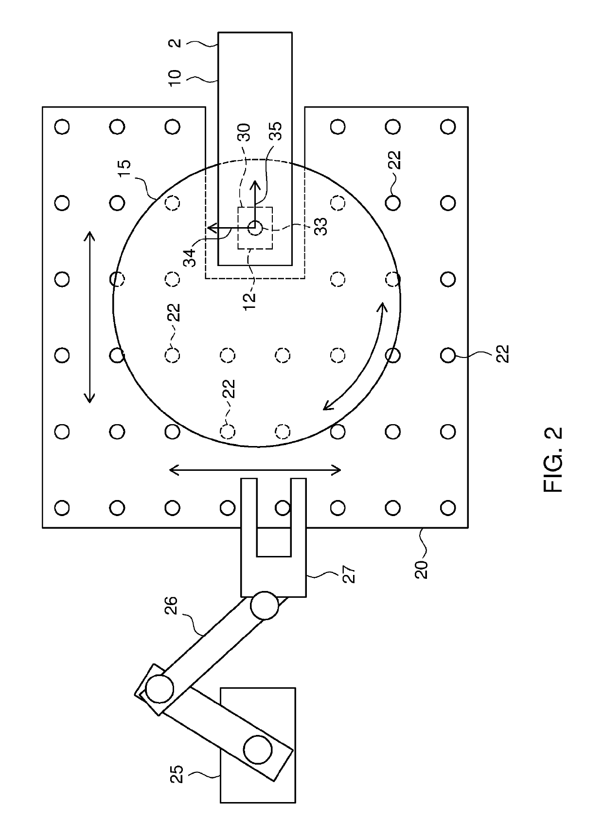
[0021]The system further comprises a sample support structure 20. The sample support structure 20...


PUM


Abstract

A scanning probe microscopy system for mapping nanostructures on a surface of a sample, comprises a metrology frame, a sensor head including a probe tip, and an actuator for scanning the probe tip relative to the sample surface. The system comprises a clamp for clamping of the sample, which clamp is fixed to the metrology frame and arranged underneath the sensor head. The clamp is arranged for locally clamping of the sample in a clamping area underneath the probe tip, the clamping area being smaller than a size of the sample such as to clamp only a portion of the sample. Moreover, a metrology frame for use in scanning probe microscopy system as described includes a clamp for clamping of a sample, wherein the clamp is fixed to the metrology frame such as to be arranged underneath the sensor head.

Description

CROSS-REFERENCE TO RELATED APPLICATIONS[0001]This patent application is a U.S. National Phase of PCT International Application No. PCT / NL2016 / 050517, filed Jul. 14, 2016, which claims priority to European Application No. 15176899.1, filed Jul. 15, 2015, which are both expressly incorporated by reference in their entireties, including any references contained therein.FIELD OF THE INVENTION[0002]The present invention is directed at a scanning probe microscopy system for mapping nanostructures on a surface of a sample, the system comprising a metrology frame, a sample support structure for supporting a sample, a sensor head including a probe tip, and an actuator for scanning the probe tip relative to the sample surface for mapping of the nanostructures. The invention is further directed at a metrology frame for use in a system as above.BACKGROUND[0003]The present document relates to scanning probe microscopy systems (SPM), such as atomic force microscopy systems (AFM). In conventional ...

Claims


Application Information

Patent Timeline
Patent Type & Authority Patents(United States)
IPC IPC(8): G01Q30/20G01Q70/04
CPCG01Q70/04G01Q30/20
Inventor KUIPER, STEFANCROWCOMBE, WILLIAM EDWARD
Owner NEDERLANDSE ORG VOOR TOEGEPAST NATUURWETENSCHAPPELIJK ONDERZOEK TNO
Why Eureka
Try Eureka