Semiconductor device including circuit configured to be in resting state

a technology of electromagnetic field and sensor device, which is applied in the direction of memory address/allocation/relocation, solid-state device, transistor, etc., can solve the problems of limited effect in reducing increase in the power consumption of the cpu, etc., to reduce the power consumption of the sensor device, and reduce the effect of power consumption

Inactive Publication Date: 2018-07-10
SEMICON ENERGY LAB CO LTD
View PDF154 Cites 0 Cited by
  • Summary
  • Abstract
  • Description
  • Claims
  • Application Information

AI Technical Summary

Benefits of technology

[0008]Moreover, although the technique in Patent Document 1 attempts to reduce the power consumption of the sensor device by powering off the sensor portion and the wireless transmitting portion, a control portion including a CPU is not powered off. The power consumption of the CPU accounts for a large proportion of the power consumption of the entire sensor device; therefore, the above technique has only a limited effect in reducing the power consumption of the sensor device.
[0009]An object of one embodiment of the present invention is to provide a novel semiconductor device. Another object of one embodiment of the present invention is to provide a semiconductor device whose power consumption can be reduced. Another object of one embodiment of the present invention is to provide a highly reliable semiconductor device. Another object of one embodiment of the present invention is to provide a semiconductor device capable of highly accurate sensing.
[0017]According to one embodiment of the present invention, a novel semiconductor device can be provided. According to another embodiment of the present invention, a semiconductor device whose power consumption can be reduced can be provided. According to another embodiment of the present invention, a highly reliable semiconductor device can be provided. According to another embodiment of the present invention, a semiconductor device capable of highly accurate sensing can be provided.

Problems solved by technology

However, the CPU needs to operate to extract data every time sensing is performed, resulting in an increase in the power consumption of the CPU.
The power consumption of the CPU accounts for a large proportion of the power consumption of the entire sensor device; therefore, the above technique has only a limited effect in reducing the power consumption of the sensor device.

Method used


Image

  • Semiconductor device including circuit configured to be in resting state
  • Semiconductor device including circuit configured to be in resting state
  • Semiconductor device including circuit configured to be in resting state

Examples


embodiment 1

[0058]In this embodiment, a configuration example of a semiconductor device of one embodiment of the present invention will be described.

Configuration Example of Semiconductor Device

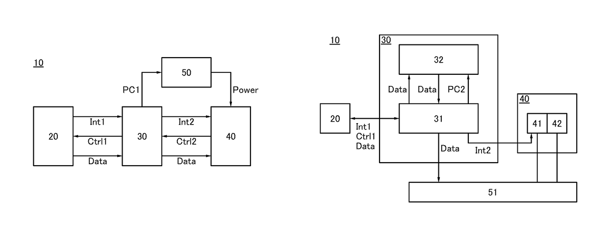
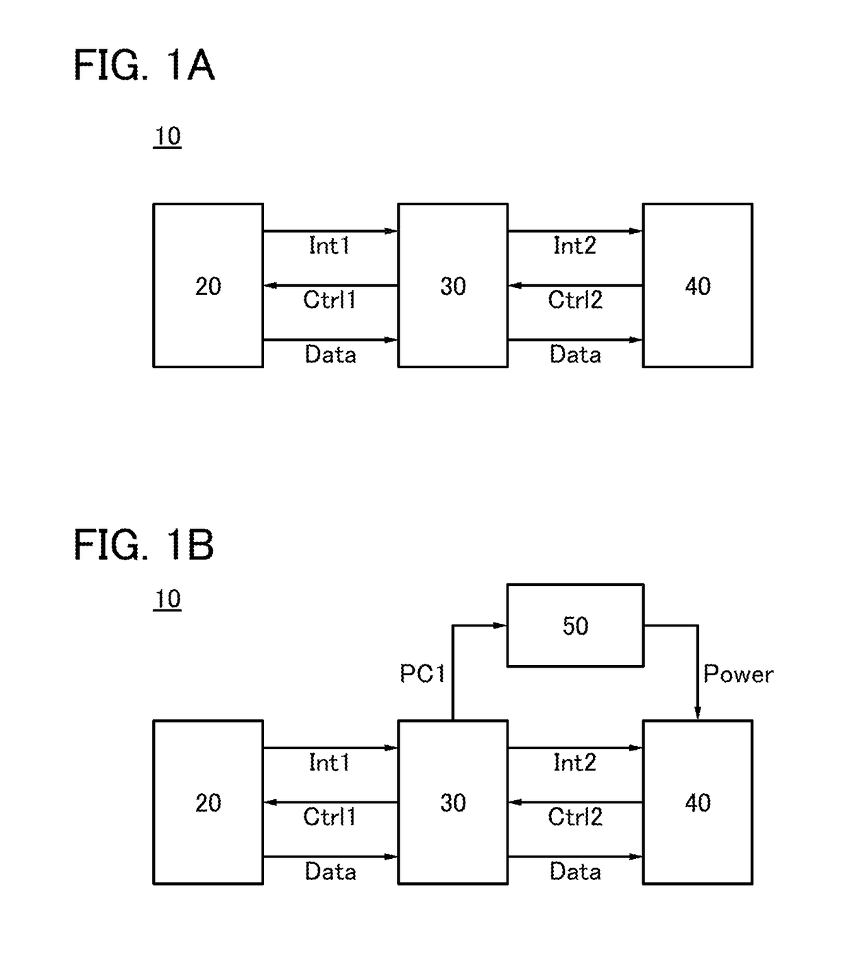
[0059]FIG. 1A illustrates a configuration example of a semiconductor device 10 of one embodiment of the present invention. The semiconductor device 10 includes a sensor portion 20, a memory portion 30, and a control portion 40. The memory portion 30 is connected to the sensor portion 20 and the control portion 40. The semiconductor device 10 can be used as a sensor device.

[0060]The sensor portion 20 is a circuit which has a function of acquiring information from the outside. Specifically, a sensor which has a function of acquiring a predetermined physical or chemical quantity can be provided in the sensor portion 20.

[0061]Here, the physical quantity refers to temperature, pressure, flow rate, light, magnetism, sound wave, speed, acceleration, humidity, current, voltage, electric field, electric power, di...

embodiment 2

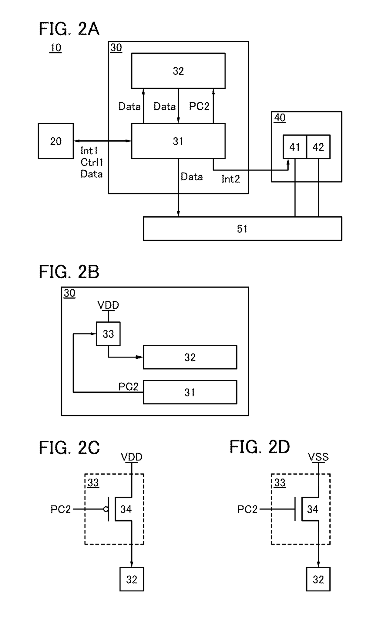
[0112]In this embodiment, a specific configuration example of the memory portion 30 of one embodiment of the present invention will be described.

Configuration Example of Control Circuit

[0113]FIG. 6 illustrates a configuration example of the control circuit 31. The control circuit 31 includes a control logic 100 and a plurality of interfaces (IF 110, IF 120, and IF 130).

[0114]The control logic 100 has a function of controlling the transmission / reception of signals to / from the sensor portion 20, the memory circuit 32, and the control portion 40. Specifically, the control logic 100 has a function of controlling the operation of the IF 110 which has functions of sending and receiving signals to and from the sensor portion 20. Furthermore, the control logic 100 has a function of controlling the operation of the IF 120 which has functions of sending and receiving signals to and from the memory circuit 32. Furthermore, the control logic 100 has functions of sending and receiving signals to...

configuration example 1

of Memory Cell

[0164]FIG. 12A illustrates a configuration example of the memory cell 311. The memory cell 311 includes a circuit 340 and a circuit 350.

[0165]The circuit 340 includes transistors 341 to 346. The transistors 341, 342, 345, and 346 are n-channel transistors, and the transistors 343 and 344 are p-channel transistors. Note that the transistors 341 and 342 may each be either an n-channel transistor or a p-channel transistor.

[0166]A gate of the transistor 341 is connected to the wiring WL. One of a source and a drain of the transistor 341 is connected to one of a source and a drain of the transistor 343, one of a source and a drain of the transistor 345, a gate of the transistor 344, and a gate of the transistor 346. The other of the source and the drain of the transistor 341 is connected to the wiring BL. A gate of the transistor 342 is connected to the wiring WL. One of a source and a drain of the transistor 342 is connected to one of a source and a drain of the transistor...


PUM


Abstract

A novel semiconductor device or a semiconductor device whose power consumption can be reduced is provided. The semiconductor device includes a sensor portion, a memory portion, and a control portion. The memory portion has functions of storing multiple detection data and sending them to the control portion. Therefore, a certain amount of detection data acquired through sensing by the sensor portion can be held, and the detection data can be sent to the control portion at a desired timing. Accordingly, in the semiconductor device, the control portion does not need to operate every time information is acquired, and thus, the power supply to the control portion can be completely or partially stopped.

Description

BACKGROUND OF THE INVENTION[0001]1. Field of the Invention[0002]One embodiment of the present invention relates to a semiconductor device, a sensor device, and an electronic device.[0003]Note that one embodiment of the present invention is not limited to the above technical field. The technical field of one embodiment of the invention disclosed in this specification and the like relates to an object, a method, or a manufacturing method. Another embodiment of the present invention relates to a process, a machine, manufacture, or a composition of matter. Another embodiment of the present invention relates to a semiconductor device, a display device, a light-emitting device, a power storage device, a memory device, a driving method thereof, or a manufacturing method thereof.[0004]2. Description of the Related Art[0005]In recent years, a variety of sensors for various applications have been provided, and these sensors are used in a wide range of electronic devices. A size reduction, a p...

Claims


Application Information

Patent Timeline
Patent Type & Authority Patents(United States)
IPC IPC(8): G06F12/02H02J1/00H02J13/00H01L27/06H01L27/11H01L27/1156
CPCG06F12/02H02J1/00H02J13/0003H01L27/1156H01L27/0688H01L27/1104H02J13/00017H10B10/12H10B41/70
Inventor TSUTSUI, NAOAKI
Owner SEMICON ENERGY LAB CO LTD
Why Eureka
Try Eureka