Semiconductor device, sensor device, and electronic device
Inactive Publication Date: 2016-06-23
SEMICON ENERGY LAB CO LTD
3 Cites 7 Cited by
AI-Extracted Technical Summary
Problems solved by technology
However, the CPU needs to operate to extract data every time sensing is performed, resulting in an increase in the power consumption of the CPU.
The power consumption of the CPU accounts f...
Benefits of technology
[0008]Moreover, although the technique in Patent Document 1 attempts to reduce the power consumption of the sensor device by powering off the sensor portion and the wireless transmitting portion, a control portion including a CPU is not powered off. The power consumption of the CPU accounts for a large proportion of the power consumption of the entire sensor device; therefore, the above technique has only a limited effect in reducing the power consumption of the sensor device...
Abstract
A novel semiconductor device or a semiconductor device whose power consumption can be reduced is provided. The semiconductor device includes a sensor portion, a memory portion, and a control portion. The memory portion has functions of storing multiple detection data and sending them to the control portion. Therefore, a certain amount of detection data acquired through sensing by the sensor portion can be held, and the detection data can be sent to the control portion at a desired timing. Accordingly, in the semiconductor device, the control portion does not need to operate every time information is acquired, and thus, the power supply to the control portion can be completely or partially stopped.
Application Domain
TransistorDc network circuit arrangements +6
Technology Topic
EngineeringTime information +4
Image
Examples
- Experimental program(11)
Example
Embodiment 1
[0058]In this embodiment, a configuration example of a semiconductor device of one embodiment of the present invention will be described.
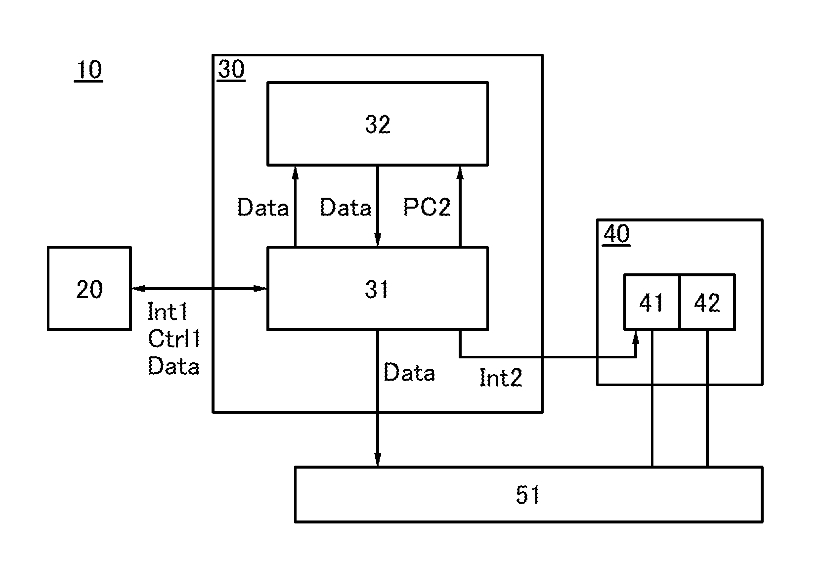
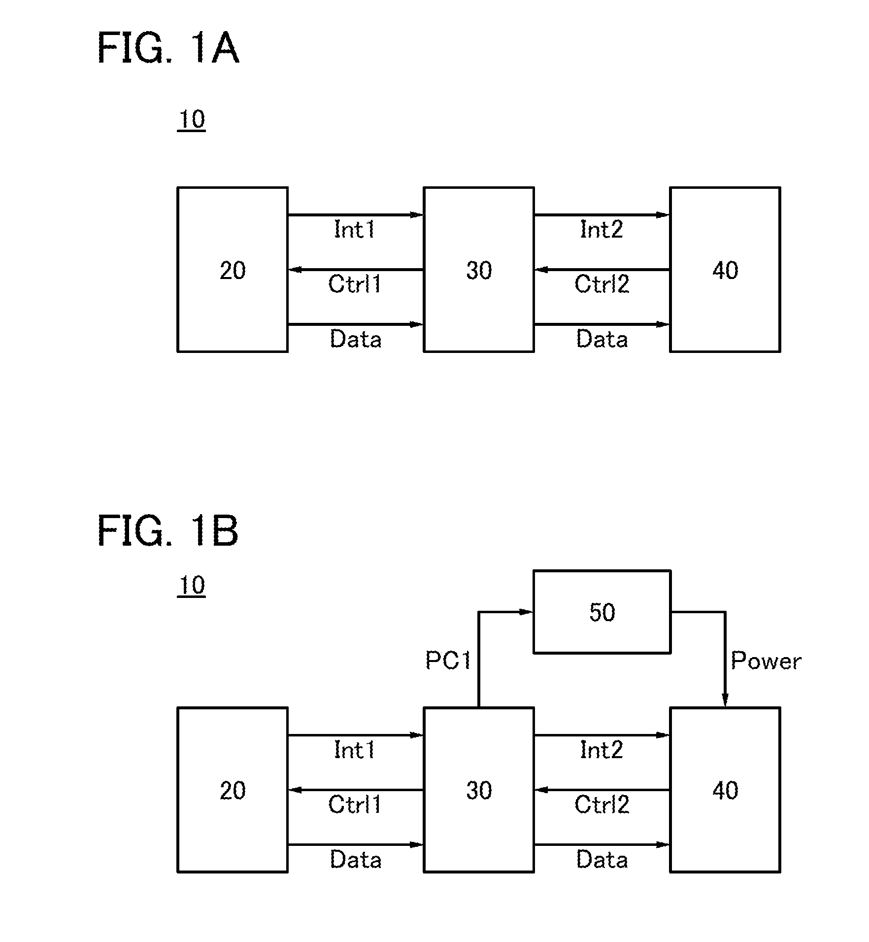
[0059]FIG. 1A illustrates a configuration example of a semiconductor device 10 of one embodiment of the present invention. The semiconductor device 10 includes a sensor portion 20, a memory portion 30, and a control portion 40. The memory portion 30 is connected to the sensor portion 20 and the control portion 40. The semiconductor device 10 can be used as a sensor device.
[0060]The sensor portion 20 is a circuit which has a function of acquiring information from the outside. Specifically, a sensor which has a function of acquiring a predetermined physical or chemical quantity can be provided in the sensor portion 20.
[0061]Here, the physical quantity refers to temperature, pressure, flow rate, light, magnetism, sound wave, speed, acceleration, humidity, current, voltage, electric field, electric power, distance, angle, or the like. The chemical quantity refers to the amount of a gaseous chemical substance such as a gas, a liquid chemical substance such as an ion, or the like. The chemical quantity further includes the amount of an organic compound such as a certain biological material contained in blood, sweat, urine, or the like. In order to acquire a chemical quantity, the sensor portion 20 selectively detects a specific substance; therefore, a substance which reacts with the substance to be detected is preferably provided in the sensor portion 20 in advance. For example, in the case of detecting a biological material or a drug, it is preferable that an enzyme, an antibody molecule, a microbial cell, or the like which reacts with the biological material or drug to be detected be subjected to polymer immobilization or the like and provided in the sensor portion 20.
[0062]Examples of the sensor which can be provided in the sensor portion 20 include a temperature sensor, a humidity sensor, a strain sensor, a thermal flow sensor, a photosensor, a gas sensor, a pressure sensor, a displacement sensor, an acceleration sensor, a flow rate sensor, a rotation sensor, a density sensor, a gyroscope, an ultrasonic sensor, a fiber optic sensor, a biosensor, an odor sensor, a taste sensor, an iris sensor, a fingerprint sensor, a palm print sensor, and a vein sensor. Microelectromechanical systems (MEMS) may also be used for the sensor provided in the sensor portion 20.
[0063]The sensor portion 20 may have a function of acquiring biological information. Examples of the biological information include body temperature, blood pressure, pulse rate, the amount of sweat, lung capacity, blood sugar level, blood alcohol concentration, the number of white blood cells, the number of red blood cells, the number of platelets, hemoglobin concentration, hematocrit level, GOT(AST) level, GPT(ALT) level, γ-GTP level, LDL cholesterol level, HDL cholesterol level, and neutral fat level. The sensor portion 20 having a function of acquiring such biological information enables the semiconductor device 10 to be used as a healthcare system.
[0064]Note that the sensor portion may include two or more kinds of sensors.
[0065]The memory portion 30 has a function of storing data corresponding to the information acquired by the sensor portion 20 (hereinafter, such data is also referred to as detection data). Specifically, when the sensor portion 20 acquires information, an interrupt signal Int1 is sent from the sensor portion 20 to the memory portion 30. When the memory portion 30 receives the signal Int1, a control signal Ctrl1 is output from the memory portion 30 to the sensor portion 20. Then, in accordance with an instruction included in the signal Ctrl1, detection data Data is sent from the sensor portion 20 to the memory portion 30 and stored in the memory portion 30. Note that the signal Int1, the signal Ctrl1, and the detection data Data can be sent or received through a serial peripheral interface (SPI) or the like.
[0066]Here, the memory portion 30 has functions of storing multiple detection data and sending them to the control portion 40. Therefore, the memory portion 30 can hold a certain amount of detection data acquired through sensing by the sensor portion 20 and send it to the control portion 40 at a desired timing. Specifically, when the amount of detection data Data stored in the memory portion 30 reaches a predetermined reference value, an interrupt signal Int2 is sent from the memory portion 30 to the control portion 40. When the control portion 40 receives the signal Int2, a control signal Ctrl2 is output from the control portion 40 to the memory portion 30. Then, in accordance with an instruction included in the signal Ctrl2, the detection data Data is sent from the memory portion 30 to the control portion 40 and processed in the control portion 40. In this manner, the memory portion 30 has functions of accumulating and storing a certain amount of detection data Data and sending it as a batch to the control portion 40.
[0067]The control portion 40 is a circuit which has a function of performing various kinds of processing such as arithmetic operation with the use of the detection data which is acquired by the sensor portion 20 and input from the memory portion 30. The control portion 40 can include a CPU, a power management unit (PMU), a memory circuit, a clock signal generation circuit, and the like.
[0068]In the case where information acquired by the sensor portion 20 is directly sent to the control portion 40, the control portion 40 (e.g., the CPU in particular) needs to operate to extract detection data every time the sensor portion 20 acquires information. As a result, the power consumption of the control portion 40 is increased. In contrast, in one embodiment of the present invention, since a certain amount of detection data can be accumulated in the memory portion 30, the control portion 40 does not need to operate every time information is acquired; thus, a period in which the power supply to the control portion 40 is completely or partially stopped can be provided. Accordingly, the power consumption of the control portion 40 can be reduced. Hereinafter, the state in which the power supply to the control portion 40 is completely or partially stopped is also referred to as a resting state of the control portion 40, and the period in which the control portion 40 is in the resting state is also referred to as a resting period of the control portion 40.
[0069]Note that the resting period of the control portion 40 may be part of or the entire period in which the amount of detection data accumulated in the memory portion 30 is below a certain reference value.
[0070]As illustrated in FIG. 1B, the semiconductor device 10 can be provided with a battery 50. The battery 50 has a function of supplying power to the control portion 40 in accordance with a control signal PC1 output from the memory portion 30.
[0071]FIG. 2A illustrates a specific configuration example of the memory portion 30 and the control portion 40. The memory portion 30 includes a control circuit 31 and a memory circuit 32. The control portion 40 includes a PMU 41 and a CPU 42. Note that the control circuit 31 is connected to the PMU 41 and the CPU 42 through a BUS 51.
[0072]The control circuit 31 has a function of reading out detection data. Specifically, the control circuit 31 has a function of reading out the detection data Data from the sensor portion 20 by outputting the signal Ctrl1 to the sensor portion 20 when receiving the signal Int1.
[0073]Furthermore, the control circuit 31 has a function of controlling the operation of the memory circuit 32. Specifically, the control circuit 31 has a function of writing the detection data Data from the sensor portion 20 to the memory circuit 32. In addition, the control circuit 31 has functions of reading out the detection data Data stored in the memory circuit 32 and outputting it to the control portion 40 through the BUS 51.
[0074]In the case where the amount of detection data Data stored in the memory circuit 32 is below the predetermined reference value, the detection data Data is accumulated in the memory circuit 32 without being read out. When the amount of detection data Data stored in the memory circuit 32 reaches the predetermined reference value, the detection data Data stored in the memory circuit 32 is read out by the control circuit 31 and output to the control portion 40.
[0075]Specifically, when the amount of detection data Data stored in the memory circuit 32 reaches the predetermined amount, the signal Int2 is input from the control circuit 31 to the PMU 41. When the interrupt signal Int2 is input to the PMU 41, power is supplied to the CPU 42. Then, the predetermined amount of detection data Data stored in the memory circuit 32 is read out by the control circuit 31 and output to the CPU 42 through the BUS 51. Note that the BUS 51 can be formed using a wiring, switch, and the like. Note that the signal Int2 may be input to the PMU 41 directly from the control circuit 31 or through the BUS 51.
[0076]The control circuit 31 may also have a function of controlling the power supply to the memory circuit 32. In the case where neither the sensing by the sensor portion 20 nor the reading of the detection data Data by the control circuit 31 is performed, no writing/reading operation is performed in the memory circuit 32. In such a period, it is preferable to supply a control signal PC2 from the control circuit 31 to the memory circuit 32 to stop the power supply to the memory circuit 32 completely or partially. Accordingly, the power consumption of the memory circuit 32 can be reduced. Hereinafter, the state in which the power supply to the memory circuit 32 is completely or partially stopped is also referred to as a resting state of the memory circuit 32, and the period in which the memory circuit 32 is in the resting state is also referred to as a resting period of the memory circuit 32.
[0077]Note that the resting period of the memory circuit 32 may be part of or the entire period in which no wiring/reading operation is performed in the memory circuit 32.
[0078]FIG. 2B illustrates a configuration in which a switch circuit 33 capable of stopping the power supply to the memory circuit 32 is provided. The control circuit 31 has a function of controlling the operation of the switch circuit 33. Specifically, the control circuit 31 has a function of controlling the conducting state of the switch circuit 33 by outputting the control signal PC2 to the switch circuit 33.
[0079]When the switch circuit 33 is turned on with the control signal PC2, a power supply potential is supplied from a power supply line VDD to the memory circuit 32 through the switch circuit 33. Thus, the writing/reading of detection data can be performed in the memory circuit 32. When the switch circuit 33 is turned off, the supply of the power supply potential to the memory circuit 32 is stopped. Thus, the memory circuit 32 can be brought into the resting state.
[0080]FIG. 2C illustrates an example in which the switch circuit 33 is formed using a transistor 34. In the example in FIG. 2C, the transistor 34 is a p-channel transistor, and the power supply line is a high-potential power supply line VDD; alternatively, as illustrated in FIG. 2D, the transistor 34 may be an n-channel transistor, and the power supply line may be a low-potential power supply line VSS.
[0081]A gate of the transistor 34 is connected to a wiring to which the control signal PC2 is input, one of a source and a drain of the transistor 34 is connected to the power supply line, and the other of the source and the drain of the transistor 34 is connected to the memory circuit 32. In FIG. 2C, when a high-level potential is supplied to the gate of the transistor 34 as the control signal PC2, the transistor 34 is turned off. In FIG. 2D, when a low-level potential is supplied to the gate of the transistor 34 as the control signal PC2, the transistor 34 is turned off. Thus, the power supply to the memory circuit 32 is stopped.
[0082]Note that a transistor whose channel formation region includes an oxide semiconductor (hereinafter also referred to as an OS transistor) can be used as the transistor 34. The OS transistor has much lower off-state current than a transistor whose channel formation region includes silicon (hereinafter also referred to as a Si transistor) or the like. Therefore, with the use of the OS transistor as the transistor 34, the power supplied to the memory circuit 32 in a period in which the transistor 34 is in the off state can be minimized, so that the power consumption can be reduced. Note that the OS transistor will be described in detail in Embodiments 2 to 4.
[0083]Note that the transistor 34 is not limited to the OS transistor. For example, a transistor whose channel formation region is formed in part of a substrate including a single crystal semiconductor can be used. As the substrate including a single crystal semiconductor, a single crystal silicon substrate, a single crystal germanium substrate, or the like can be used.
[0084]The transistor 34 can be a transistor whose channel formation region is formed in a semiconductor film including a material other than an oxide semiconductor. For example, a transistor whose channel formation region includes a semiconductor which is a non-single-crystal semiconductor and is not an oxide semiconductor can be used. Examples of such a non-single-crystal semiconductor include non-single-crystal silicon such as amorphous silicon, microcrystalline silicon, or polycrystalline silicon and non-single-crystal germanium such as amorphous germanium, microcrystalline germanium, or polycrystalline germanium.
[0085]Note that the transistors listed above can also be used as transistors in the following description.
[0086]The memory circuit 32 has a function of storing multiple detection data Data. The memory circuit 32 can have a simple configuration when a first-in, first-out (FIFO) memory circuit or the like is employed. When the amount of detection data Data accumulated in the memory circuit 32 reaches a certain amount, the detection data Data is output to the CPU 42 through the BUS 51.
[0087]Here, the memory circuit 32 is preferably formed using an OS transistor. In this case, leakage of data stored in the memory circuit 32 can be minimized, and the data can be held for a long time. Therefore, even in the resting period of the memory circuit 32, data stored in the memory circuit 32 can be held for a long time. Note that a specific configuration example of the memory circuit 32 including an OS transistor will be described in detail in Embodiment 2.
[0088]The PMU 41 has a function of controlling the power supply to the CPU 42. In the period in which the amount of detection data Data stored in the memory circuit 32 is below the predetermined reference value, the detection data Data is not sent to the CPU 42, and the CPU 42 does not process the detection data. Therefore, the power supply to the CPU 42 can be completely or partially stopped. When the amount of detection data stored in the memory circuit 32 reaches the predetermined reference value, the signal Int2 is output from the control circuit 31 to the PMU 41 to restart the power supply to the CPU 42. Hereinafter, the state in which the power supply to the CPU 42 is completely or partially stopped is also referred to as a resting state of the CPU 42, and the period in which the CPU 42 is in the resting state is also referred to as a resting period of the CPU 42.
[0089]Note that the resting period of the CPU 42 may be part of or the entire period in which the amount of detection data Data stored in the memory circuit 32 is below the reference value.
[0090]The CPU 42 has a function of performing various kinds of processing such as arithmetic operation with the use of the detection data. As the PMU 41 and the CPU 42, integrated circuits each of which includes a plurality of transistors can be used. Note that the plurality of transistors can be formed using a material similar to that of the transistor 34.
[0091]As described above, in one embodiment of the present invention, in the period in which the amount of detection data accumulated in the memory circuit 32 is below a certain amount, it is unnecessary to send the detection data from the memory circuit 32 to the control portion 40 through the control circuit 31; thus, a circuit in the control portion 40 (e.g., the CPU 42 in particular) can be in the resting state. Accordingly, the power consumption of the control portion 40 can be reduced.
[0092]Next, an operation example of the semiconductor device 10 in FIGS. 1A and 1B and FIG. 2A will be described with reference to FIG. 3, FIG. 4, and FIG. 5.
[0093]FIG. 3 is a timing chart illustrating the operation of the sensor portion 20 and the memory portion 30. As an example, the operation in the case where the signal transmission/reception between the sensor portion 20 and the memory portion 30 is performed through an SPI and a clock signal CLK is input to the sensor portion 20 will be described.
[0094]First, in Period T1, sensing by the sensor portion 20 is not performed, so that the signal Int1 is not output to the memory portion 30. In Period T1, the memory circuit 32 and the CPU 42 can be in the resting state.
[0095]Next, when the sensor portion 20 acquires information, the signal Int1 is output to the memory portion 30 (Period T2). When the memory portion 30 receives the signal Int1, the signal Ctrl1 is sent from the memory portion 30 to the sensor portion 20 (Period T3 and Period T4). Note that the following operation example is illustrated here: a control signal A for selecting information that is to be read out from among a plurality of pieces of information acquired by the sensor portion 20 is sent in Period T3, and a control signal B for specifying the address of the information that is to be read out from the sensor portion 20 is sent in Period T4.
[0096]After receiving the signal Ctrl1 including the control signal A and the control signal B, the sensor portion 20 sends the detection data Data to the memory portion 30 (Period T5). Thus, the detection data Data is stored in the memory portion 30.
[0097]Through the above operation, information acquired by the sensor portion 20 is accumulated in the memory portion 30.
[0098]Next, the operation of the control circuit 31 in FIGS. 2A and 2B will be described. FIG. 4 is a flow chart illustrating the operation of the control circuit 31 in the case where the detection data from the sensor portion 20 is written to the memory circuit 32.
[0099]First, the control circuit 31 is in the standby state until an interruption occurs (Step S11). When an interruption occurs and the signal Int1 is output from the sensor portion 20 (YES in Step S12), the control circuit 31 reads out the detection data Data from the sensor portion 20 (Step S13). The detection data Data is read out in accordance with the timing chart in FIG. 3. In the standby period (Step S11), in which no interruption occurs, the memory circuit 32 and the CPU 42 can be in the resting state.
[0100]Subsequently, the control circuit 31 determines whether the memory circuit 32 is in the resting state or not (Step S14). In the case where the memory circuit 32 is in the resting state, power is supplied to the memory circuit 32 to cancel the resting state (Step S15).
[0101]Subsequently, the control circuit 31 determines whether the amount of detection data stored in the memory circuit 32 has reached the predetermined reference value or not (or whether the memory circuit 32 is in a full state or not) (Step S16). In the case where the memory circuit 32 is in the full state, the full state is canceled (Step S17). To cancel the full state, for example, the detection data Data accumulated in the memory circuit 32 is output to the outside. Note that details of the operation for canceling the full state will be described with reference to FIG. 5. After the full state is canceled, the detection data Data is written to the memory circuit 32 (Step S18).
[0102]Note that the number of detection data sets stored in the memory circuit 32 can be counted by a counter or the like.
[0103]Through the above operation, the detection data can be written to the memory circuit 32.
[0104]Next, the operation of the control circuit 31 in the case where the detection data is sent from the memory circuit 32 to the CPU 42 will be described. FIG. 5 is a flow chart illustrating this operation.
[0105]First, until the memory circuit 32 reaches the full state, the control circuit 31 is in the standby state (Step S21). When the memory circuit 32 reaches the full state (YES in Step S22), the control circuit 31 outputs an interrupt signal (signal Int2) to the PMU 41 (Step S23). In the case where the CPU 42 is in the resting state at this time, power is supplied from the PMU 41 to the CPU 42 to cancel the resting state.
[0106]When the signal Int2 is input to the PMU 41, the CPU 42 requests the control circuit 31 to read out the detection data Data (Step S24). In response to this, the control circuit 31 reads out the detection data Data from the memory circuit 32 (Step S25), and the detection data Data read out by the control circuit 31 is sent to the CPU 42 through the BUS 51 (Step S26). When the detection data Data is sent to the CPU 42, the full state of the memory circuit 32 is canceled (Step S27).
[0107]Through the above operation, a certain amount of accumulated detection data is sent to the CPU 42, so that the full state is canceled.
[0108]As described above, in one embodiment of the present invention, since a certain amount of detection data can be accumulated in the memory portion 30, the control portion 40 does not need to operate every time information is acquired; thus, the control portion can be in the resting state. Accordingly, the power consumption of the semiconductor device can be reduced.
[0109]Moreover, in one embodiment of the present invention, the memory circuit 32 can be in the resting state in the period in which no writing/reading operation is performed in the memory circuit 32. Thus, the power consumption of the semiconductor device can be reduced.
[0110]Note that the configuration of one embodiment of the present invention is not limited to that described above. In other words, since various embodiments of the invention are described in this embodiment, one embodiment of the present invention is not limited to a particular embodiment. For example, although the semiconductor device including the memory portion 30 is described as one embodiment of the present invention, depending on the situation or circumstances, one embodiment of the present invention does not necessarily include the memory portion 30. In addition, in the semiconductor device of one embodiment of the present invention, data is transmitted to the control portion 40 when a certain amount of data is accumulated in the memory portion 30; depending on the situation or circumstances, in one embodiment of the present invention, the detection data may be transmitted to the control portion 40 every time the detection data is input to the memory portion 30.
[0111]This embodiment can be combined with any of the other embodiments as appropriate. Thus, a content (or part of the content) described in this embodiment can be applied to, combined with, or replaced by a different content (or part of the different content) described in this embodiment and/or a content (or part of the content) described in another embodiment or other embodiments. In each embodiment, a content described in the embodiment is a content described with reference to a variety of diagrams or a content described with text in the specification. By combining a diagram (or part of thereof) illustrated in one embodiment with another part of the diagram, a different diagram (or part of thereof) illustrated in the embodiment, and/or a diagram (or part of thereof) illustrated in another embodiment or other embodiments, much more diagrams can be created. This also applies to other embodiments.
Example
Embodiment 2
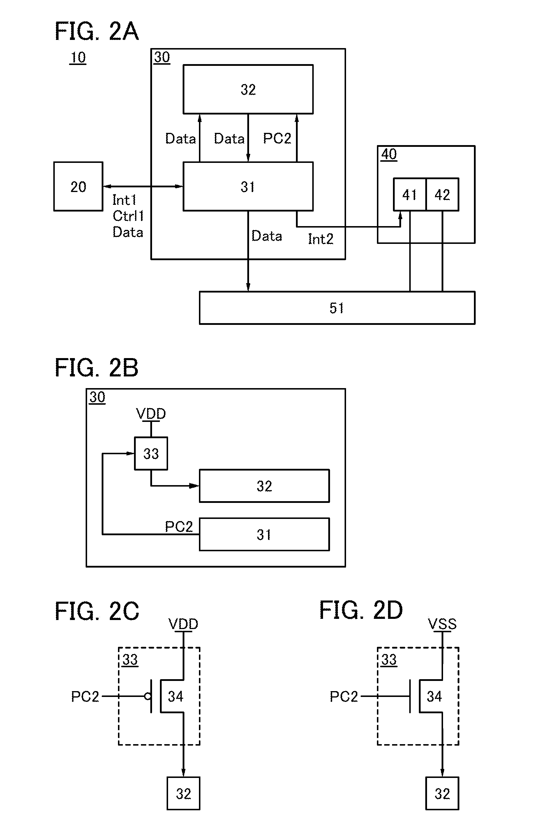
[0112]In this embodiment, a specific configuration example of the memory portion 30 of one embodiment of the present invention will be described.
[0113]FIG. 6 illustrates a configuration example of the control circuit 31. The control circuit 31 includes a control logic 100 and a plurality of interfaces (IF 110, IF 120, and IF 130).
[0114]The control logic 100 has a function of controlling the transmission/reception of signals to/from the sensor portion 20, the memory circuit 32, and the control portion 40. Specifically, the control logic 100 has a function of controlling the operation of the IF 110 which has functions of sending and receiving signals to and from the sensor portion 20. Furthermore, the control logic 100 has a function of controlling the operation of the IF 120 which has functions of sending and receiving signals to and from the memory circuit 32. Furthermore, the control logic 100 has functions of sending and receiving signals to and from the control portion 40.
[0115]The control logic 100 has a function of controlling the IF 110 as follows: when receiving the signal Int1 from the sensor portion 20, the control logic 100 outputs a control signal Ctrl3 to the IF 110, thereby controlling the reading of the detection data Data from the sensor portion 20.
[0116]The control logic 100 has a function of controlling the IF 120 by outputting a signal Ctrl4 to the IF 120, thereby controlling the writing of the detection data Data to the memory circuit 32 and the reading of the detection data Data from the memory circuit 32. The control logic 100 also has a function of controlling the power supply to the memory circuit 32 by outputting the control signal PC2 to the memory circuit 32.
[0117]The control logic 100 has a function of controlling the output of the detection data Data to the control portion 40 by outputting the signal Int2 to the control portion 40.
[0118]The IF 110 has a function of reading out the detection data Data from the sensor portion 20 by outputting the signal Ctrl1 to the sensor portion 20 in accordance with the instruction from the control logic 100. The IF 110 also has a function of outputting the read-out detection data Data to the IF 120.
[0119]The IF 120 has a function of outputting the detection data Data from the IF 110 to the memory circuit 32 in accordance with the instruction from the control logic 100. Thus, the detection data Data is written to the memory circuit 32. Furthermore, the IF 120 has a function of reading out the detection data Data stored in the memory circuit 32. The IF 120 also has a function of outputting the read-out detection data Data to the IF 130.
[0120]The IF 130 has a function of outputting the detection data Data from the IF 120 to the control portion 40 through the BUS 51.
[0121]FIG. 7 illustrates a configuration example of the memory circuit 32. The memory circuit 32 includes a memory region 200, a counter 210, a counter 220, and a comparator circuit 230.
[0122]The memory region 200 has a function of storing multiple detection data Data. The memory region 200 can be formed using any of a variety of memory circuits such as a flip-flop, a DRAM, and an SRAM.
[0123]The memory region 200 has a function of, when a signal WE is input, storing the detection data Data from the control circuit 31 at an address that is specified by a signal WADDR. The memory region 200 also has a function of outputting the detection data Data stored at an address that is specified by a signal RADDR to the control circuit 31. Note that the clock signal CLK may be input to the memory region 200.
[0124]The counter 210 has a function of counting the number of sets of detection data Data input from the control circuit 31. Specifically, the counter 210 has a function of, in the period in which the signal WE is input, counting the number of sets of detection data Data written to the memory region 200. When the number of detection data sets that is counted by the counter 210 exceeds a certain value, that is, when the memory circuit 32 reaches the full state, a signal Full is output from the comparator circuit 230.
[0125]The counter 220 has a function of counting the number of sets of detection data Data output to the control circuit 31. Specifically, the counter 220 has a function of, in a period in which a signal RD is input, counting the number of sets of detection data Data read out from the memory region 200. The comparator circuit 230 compares the number of counts obtained by the counter 210 with the number of counts obtained by the counter 220. When the numbers of counts of the counters satisfy certain conditions, a signal Empty is output from the comparator circuit 230.
[0126]The comparator circuit 230 has a function of outputting the signal Full or the signal Empty in accordance with the results of comparing the number of counts of the counter 210 with the number of counts of the counter 220.
[0127]Next, an operation example of the memory circuit 32 in FIG. 7 will be described. FIG. 8 is a timing chart illustrating the operation of the memory circuit 32. Described here is an example in which the counter 210 and the counter 220 are each a 2-bit counter.
[0128]In Period T11, the signal WE and the signal RD are at the low level, and no writing/reading of the detection data Data is performed. Therefore, the counter 210 and the counter 220 count “0”.
[0129]Subsequently, in Period T12, the signal WE is set at the high level, and the detection data Data is written. In the period in which the signal WE is at the high level, the counter 210 counts the number of sets of detection data Data written to the memory region 200. When the number of written detection data sets reaches “4”, the counter 210 counts “0”, and the signal Full which indicates that the amount of detection data stored in the memory region 200 has reached a certain amount is output from the comparator circuit 230.
[0130]Subsequently, in Period T13, the signal WE is set at the low level, so that the writing of the detection data Data is finished.
[0131]Subsequently, in Period T14, the signal RD is set at the high level, and the detection data Data is read out. In the period in which the signal RD is at the high level, the counter 220 counts the number of sets of detection data Data read out from the memory region 200. When the number of detection data sets that have been read out reaches “4”, the counter 220 counts “0”, and the signal Empty which indicates that a certain amount of detection data Data stored in the memory region 200 has been read out is output from the comparator circuit 230. Note that the detection data Data that has been read out from the memory region 200 is output to the control portion 40 through the control circuit 31 and the BUS 51 (see FIG. 2A).
[0132]Subsequently, in Period T15, the signal RD is set at the low level, so that the reading of the detection data Data is finished.
[0133]In the above-described manner, the memory circuit 32 can accumulate a certain amount of detection data Data in the memory region 200 and then send it as a batch to the control circuit 31. Therefore, in the accumulation period of the detection data Data, the reading operation of the detection data Data stored in the memory region 200 can be omitted, which allows the control portion 40 (see FIG. 2A) to stop processing the detection data Data. Accordingly, the power consumption of the control portion 40 can be reduced.
[0134]Note that the memory region 200 is preferably formed using, but not particularly limited to, a memory circuit including an OS transistor. Since the OS transistor has low off-state current, the memory region 200 including the OS transistor can hold the detection data for a long time even in a period in which power is not supplied. Therefore, even in the resting period of the memory circuit 32, the detection data can be held for a long time. A configuration example of the memory region 200 including the OS transistor will be described below.
Example
[Configuration Example 1 of Memory Region]
[0135]FIG. 9 illustrates a configuration example of the memory region 200. The memory region 200 in FIG. 9 includes a plurality of flip-flops 300, a decoder 301, an AND circuit 302, and a multiplexer 303. In the configuration illustrated here, data of 4 bits×4 can be stored in the flip-flops 300 in 4 rows×4 columns; however, the number of flip-flops 300 is not limited thereto and may be a given number.
[0136]The decoder 301 has a function of outputting, in accordance with the external input signal WADDR, a signal for selecting the flip-flop 300 to which data is to be written. In the case where the signal WADDR is not coded and can be directly input to the flip-flop 300, the decoder 301 can be omitted.
[0137]The signal WE is input to a first input terminal of the AND circuit 302, and the signal CLK is input to a second input terminal of the AND circuit 302. When the signal WE is set at the high level, a clock signal is output from an output terminal of the AND circuit 302.
[0138]The detection data is written to the flip-flop 300 through the following operation. First, the signal WADDR is decoded by the decoder 301, and a flip-flop to which the detection data Data is to be written is selected. After that, the signal WE is set at the high level, so that the clock signal is input to the flip-flop 300. Thus, the detection data Data is stored in the predetermined flip-flop 300.
[0139]The detection data Data is read out from the flip-flop 300 in the following manner: the signal RADDR for specifying the address at which the reading of the detection data Data is to be performed is input to the multiplexer 303, so that a predetermined flip-flop 300 is selected, and the detection data is output from the selected flip-flop 300 through the multiplexer 303.
[0140]Here, the memory region 200 which includes the flip-flop 300 in combination with an OS transistor can hold the detection data for a long time even in a period in which power is not supplied. FIG. 10 illustrates a configuration example in which an OS transistor is connected to the flip-flop 300.
[0141]The memory region 200 in FIG. 10 includes the flip-flop 300, a transistor 304, a transistor 305, a transistor 306, a capacitor 307, and a selection circuit 308. Here, the transistors 304 to 306 are OS transistors.
[0142]A gate of the transistor 304 is connected to a terminal BK, one of a source and a drain of the transistor 304 is connected to a terminal SD_IN, and the other of the source and the drain of the transistor 304 is connected to a node SD. A gate of the transistor 305 is connected to a terminal RE, one of a source and a drain of the transistor 305 is connected to a node N1, and the other of the source and the drain of the transistor 305 is connected to the node SD. A gate of the transistor 306 is connected to the terminal BK, one of a source and a drain of the transistor 306 is connected to the node N1, and the other of the source and the drain of the transistor 306 is connected to a terminal Q. One electrode of the capacitor 307 is connected to the node N1, and the other electrode of the capacitor 307 is connected to a terminal to which a predetermined potential is supplied. The selection circuit 308 is connected to the node SD, a terminal D, a terminal SE, and the flip-flop 300. An operation example of the flip-flop 300 in FIG. 10 will be described below.
[0143]In normal operation of the flip-flop 300, a power supply potential and a clock signal are supplied to the flip-flop 300. When the detection data Data is written to the flip-flop 300, the detection data Data is input to the terminal D. Here, the potentials of the terminal RE and the terminal BK are at the low level; therefore, the transistors 304 to 306 are in the off state. The terminal SE is also at the low level, and the selection circuit 308 is conducting between the terminal D and the flip-flop 300. Note that the clock signal is input to the terminal CLK.
[0144]The detection data Data is read out in such a manner that the data stored in the flip-flop 300 is output through the terminal Q to the multiplexer 303 (see FIG. 9).
[0145]In this manner, in the period in which the data writing/reading is performed in the flip-flop 300, the flip-flop 300 is supplied with the power supply potential and the clock signal and operates normally. Hereinafter, the state in which the flip-flop 300 operates normally is also referred to as an active mode.
[0146]In a period in which no data writing/reading or the like is performed in the flip-flop 300, that is, a period in which the flip-flop 300 does not need to operate, the supply of the power supply potential or the clock signal is stopped in the following manner.
[0147]First, the potential of the terminal BK is set to the high level to turn on the transistor 306. Accordingly, electrical continuity is established between the terminal Q, which corresponds to an output terminal of the flip-flop 300, and the node N1. That is, output data of the flip-flop 300 is transmitted to the node N1. After that, the potential of the terminal BK is set to the low level to turn off the transistor 306. Accordingly, the node N1 is brought into the floating state, so that the output data of the flip-flop 300 is held at the node N1.
[0148]Thus, data can be backed up in such a manner that data stored in the flip-flop 300 is moved to the node N1 and held. Furthermore, in the period in which the data is stored at the node N1, the supply of the power supply potential or the clock signal to the flip-flop 300 can be stopped. Accordingly, the power consumption of the flip-flop 300 can be reduced. Hereinafter, the state in which the supply of the power supply potential or the clock signal to the flip-flop 300 is stopped is also referred to as a sleep mode.
[0149]Moreover, since the transistors 305 and 306 are OS transistors, their off-state current is extremely low. Therefore, in a period in which the potentials of the gates of the transistors 305 and 306 are at the low level, the potential of the node N1 can be held for a long time.
[0150]In the case where the flip-flop 300 returns from the sleep mode to the active mode, the supply of the power supply potential, data restoring, and the supply of the clock signal are performed in the following manner.
[0151]First, the power supply potential is supplied to the flip-flop 300. After that, the potential of the terminal RE is set to the high level to turn on the transistor 305. Accordingly, electrical continuity is established between the node N1 and the node SD, so that the data that has been moved to the node N1 is transmitted to the node SD. The potential of the terminal SE is also set to the high level, so that electrical continuity is established between the node SD and an input terminal of the flip-flop 300 through the selection circuit 308; thus, the data that has been moved to the node N1 is input to the input terminal of the flip-flop 300.
[0152]Subsequently, the clock signal is supplied from the terminal CLK to the flip-flop 300 for a certain period of time. Consequently, data is written to the flip-flop 300, and the flip-flop 300 returns to the state immediately before the sleep mode. After that, the potentials of the terminal SE and the terminal RE are set to the low level. Accordingly, electrical continuity is established between the terminal D and the input terminal of the flip-flop 300. In addition, the transistor 305 is turned off, so that the node N1 is brought into the floating state.
[0153]After a certain period of time since the potentials of the terminal SE and the terminal RE have been set to the low level, the input of the clock signal is restarted to set the flip-flop 300 in the active mode.
[0154]In the above-described manner, the OS transistors connected to the flip-flop 300 make it possible to stop the supply of the power supply potential or the clock signal to the flip-flop 300.
[0155]In the case where the amount of power needed for the switching from the sleep mode to the active mode is larger than the amount of power which can be saved by stopping the supply of the power supply potential to the flip-flop 300, it is preferable, in the sleep mode, to stop only the supply of the clock signal and not to stop the supply of the power supply potential.
[0156]Moreover, when a plurality of circuits having the configuration of the memory region 200 in FIG. 10 is connected in series to form a scan chain, a scan test can be conducted. Specifically, the potential of the terminal RE is set to the low level to turn off the transistor 305, and the potential of the terminal BK is set to the high level to turn on the transistors 304 and 306. In addition, a high-level signal is supplied to the terminal SE to establish electrical continuity between the node SD and the input terminal of the flip-flop 300. Accordingly, the output data of the flip-flop 300 is input to the terminal SD_IN of the circuit in the next stage.
[0157]Subsequently, scan test data SCNIN is input to the terminal SD_IN of the circuit in the first stage of the scan chain. Shift operation in the scan chain is performed by inputting a clock signal, and SCNIN is written to the flip-flops 300 in the scan chain. Then, normal operation of the flip-flops 300 is performed, and output data of the logic circuit is held in the flip-flops 300. The mode is set to the scan mode again to perform the shift operation in the scan chain. Whether the logic circuit and the flip-flops 300 fail to operate properly can be determined from data output from the flip-flop 300 in the last stage.
PUM


Description & Claims & Application Information
We can also present the details of the Description, Claims and Application information to help users get a comprehensive understanding of the technical details of the patent, such as background art, summary of invention, brief description of drawings, description of embodiments, and other original content. On the other hand, users can also determine the specific scope of protection of the technology through the list of claims; as well as understand the changes in the life cycle of the technology with the presentation of the patent timeline. Login to view more.
Similar technology patents
Semiconductor device including capacitorless ram
Owner:LONGITUDE LICENSING LTD
Efficient route update protocol for wireless sensor network
Owner:SAMSUNG ELECTRONICS CO LTD +1
Semiconductor circuit, method for driving the same, storage device, register circuit, display device, and electronic device
Owner:SEMICON ENERGY LAB CO LTD
Method and system of unmanned plane omnibearing obstacle avoidance based on binocular vision
Owner:SHENZHEN AUTEL INTELLIGENT AVIATION TECH CO LTD
Classification and recommendation of technical efficacy words
- accurately sense
- reduce power consumption
Robot arm including force sensing apparatus
ActiveUS20130110289A1accurately sense
Owner:SAMSUNG ELECTRONICS CO LTD
Pressure sensor with improved strain gauge
Owner:SENSATA TECHNOLOGIES INC
Motor shaft state detection method, motor control method, motor shaft state detection device, motor control device, vehicle height adjustment device, saddle-type vehicle
PendingUS20220203795A1accurately sense
Owner:HITACHI ASTEMO LTD
Electrode array for use in medical stimulation and methods thereof
Owner:CASE WESTERN RESERVE UNIV
Method of placing and routing for power optimization and timing closure
Owner:GOLDEN GATE TECH
Method of reselecting a cell based on priorities
Owner:LG ELECTRONICS INC
Organic light-emitting devices with mixed electron transport materials
Owner:EASTMAN KODAK CO