Supercharge Your Innovation With Domain-Expert AI Agents!

Template for imprint lithography and methods of making and using the same

a technology of imprint lithography and template, which is applied in the field of imprint lithography, can solve the problems of complex components formed during electronic device fabrication on the wafer, requiring complex extra processing, and not being able to achieve the exposed surface along a single plan

Active Publication Date: 2020-03-31
CANON KK
View PDF26 Cites 0 Cited by
  • Summary
  • Abstract
  • Description
  • Claims
  • Application Information

AI Technical Summary

Benefits of technology

The patent describes a template for imprint lithography that includes tiers with features. The features have depths and heights within a certain range. The first and second tiers have corresponding surfaces at the same elevation. The features can also have different depths and heights in different parts of the template. The template can be recessed deeper into the first tier. The method of making the template involves patterning the template to define the tiers and features. The template can be used to create patterns on a substrate for making electronic devices. The substrate can have a nonplanar surface or a different elevation in different regions. The template can also have an exclusion zone. The method can include using a sacrificial layer and a formable material to create the patterns. The technical effects of the patent are the improved precision and accuracy of the features created using the template, as well as the ability to create patterns on nonplanar surfaces or in different regions of the substrate.

Problems solved by technology

Patterns of components being formed during fabrication of electronic devices on the wafer are becoming more complex.
The combination of smaller device sizes and more elevational issues provide many challenges to lithographic processes.
However, an exposed surface along a single plane may not be achievable or require complex extra processing to make the exposed surface planar.

Method used


Image

  • Template for imprint lithography and methods of making and using the same
  • Template for imprint lithography and methods of making and using the same
  • Template for imprint lithography and methods of making and using the same

Examples


Embodiment Construction

[0050]The following description in combination with the figures is provided to assist in understanding the teachings disclosed herein. The following discussion will focus on specific implementations and embodiments of the teachings. This focus is provided to assist in describing the teachings and should not be interpreted as a limitation on the scope or applicability of the teachings.

[0051]The term “device layer” is intended to mean a layer of device substrate. Examples of device layers include conductive layers, semiconductor layers, and insulating layers. Such layers may be parts of electronic components of an electronic device formed on or within the device substrate.

[0052]The term “device substrate” is intended to mean a substrate from which electronic devices may be formed. The device substrate may include a semiconductor base material but may include an insulating base material, such as a glass, sapphire, spinel, or the like. The device substrate may be in the form of a wafer....


PUM

PropertyMeasurementUnit
active areaaaaaaaaaaa
widthaaaaaaaaaa
depthsaaaaaaaaaa

Abstract

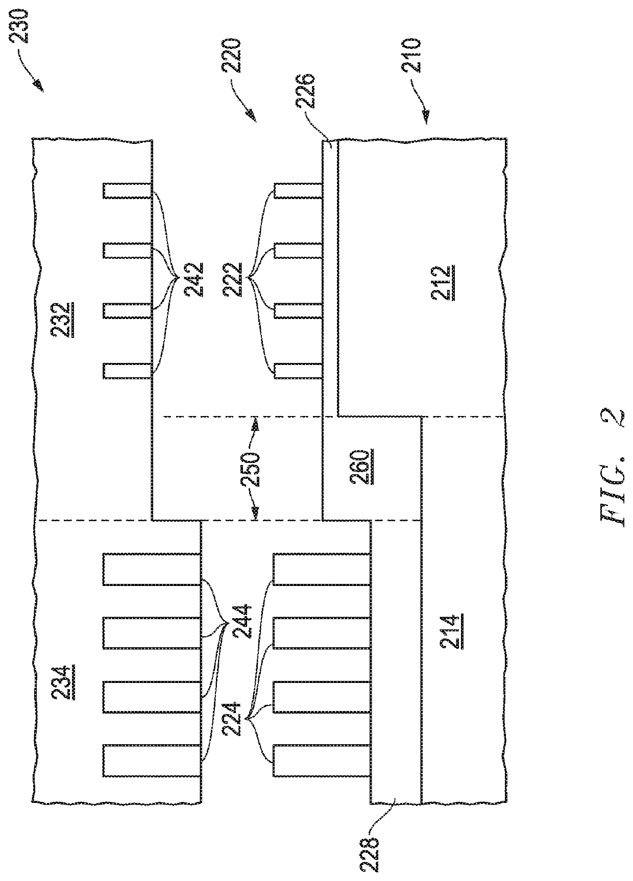
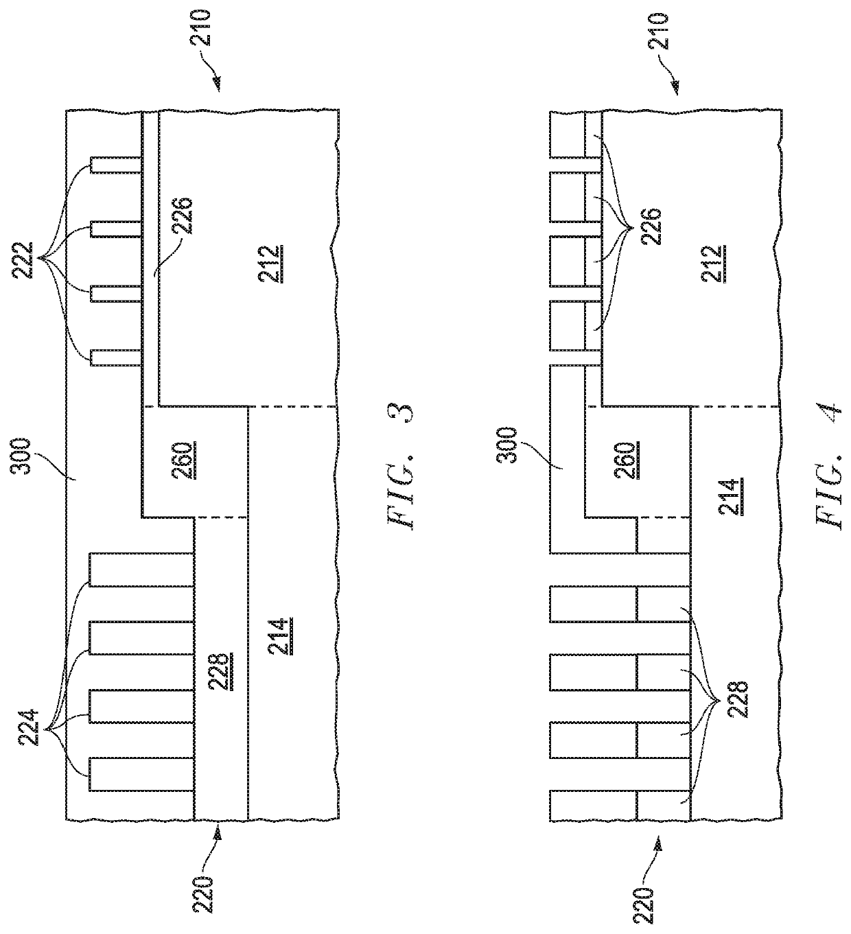
A template for imprint lithography can include an active area that includes a plurality of tiers including a first tier and a second tier, and a first feature within the first tier or the second tier. In another embodiment, the first and second tiers include features, and the average feature depth or height within the first tier may be substantially the same as or different from the average feature depth or height within the second tier. The template can be used in imprinting a formable layer to form a patterned resist layer over a device substrate that has at least two tiers. The template and its use are well suited for device substrates having exposed surfaces at significantly different elevations, particularly where planarization would be complicated or nearly impossible to implement.

Description

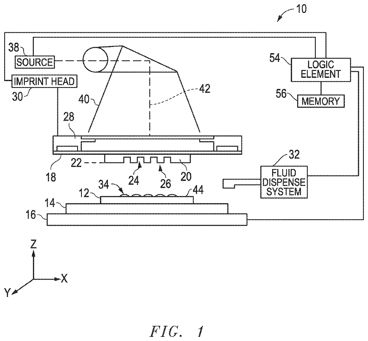
FIELD OF THE DISCLOSURE[0001]The present disclosure relates to imprint lithography, and more particularly to templates for imprint lithography applications and methods of making and using such templates.RELATED ART[0002]Imprint lithography apparatuses and processes are useful in forming nanoscale patterns on semiconductor wafers in the fabrication of electronic devices. Such apparatuses and processes can include the use of fluid dispense systems for depositing a formable material, for example, a polymerizable material, such as a resin or a resist layer, onto the wafer, using techniques such as fluid droplet dispense. The dispensed material is contacted with an imprint template (or mold) having desired pattern features and then solidified, forming a patterned layer on the wafer.[0003]Patterns of components being formed during fabrication of electronic devices on the wafer are becoming more complex. Exposed surfaces of the substrate can lie at different elevations. An example of such ...

Claims


Application Information

Patent Timeline
Patent Type & Authority Patents(United States)
IPC IPC(8): G03F7/00H01L21/027H01L21/67H01L27/105
CPCH01L21/0271G03F7/0002H01L21/67092H01L21/6715H01L27/1052H10B99/00
Inventor ECKERT, ANDREW R.
Owner CANON KK
Features
  • R&D
  • Intellectual Property
  • Life Sciences
  • Materials
  • Tech Scout
  • Unparalleled Data Quality
  • Higher Quality Content
  • 60% Fewer Hallucinations
Learn More