Supercharge Your Innovation With Domain-Expert AI Agents!

Three dimensional memory device fabricating method and applications thereof

a three-dimensional memory and fabrication method technology, applied in the field of memory devices, can solve the problems of limited scaling capability, high parallel programming, and inconvenient operation, and achieve the effect of improving the retention reliability of the three-dimensional memory devi

Active Publication Date: 2020-07-28
MACRONIX INT CO LTD
View PDF5 Cites 2 Cited by
  • Summary
  • Abstract
  • Description
  • Claims
  • Application Information

AI Technical Summary

Benefits of technology

The patent describes a new design for a 3D memory device that prevents problems such as sneak paths during programming. The design also improves the reliability of the memory device by using a floating gate.

Problems solved by technology

For example, it has limited scaling capability (a limited memory density much below 1 Gb) thus is not cost effective.
Besides, the programming current of ReRAM or PCM is high (>50 uA for each cell) thus does not allow highly parallel programming; and the resistor devices of ReRAM or PCRAM are often highly non-linear with respect to the applied bias which makes analog computing difficult.

Method used


Image

  • Three dimensional memory device fabricating method and applications thereof
  • Three dimensional memory device fabricating method and applications thereof
  • Three dimensional memory device fabricating method and applications thereof

Examples


Embodiment Construction

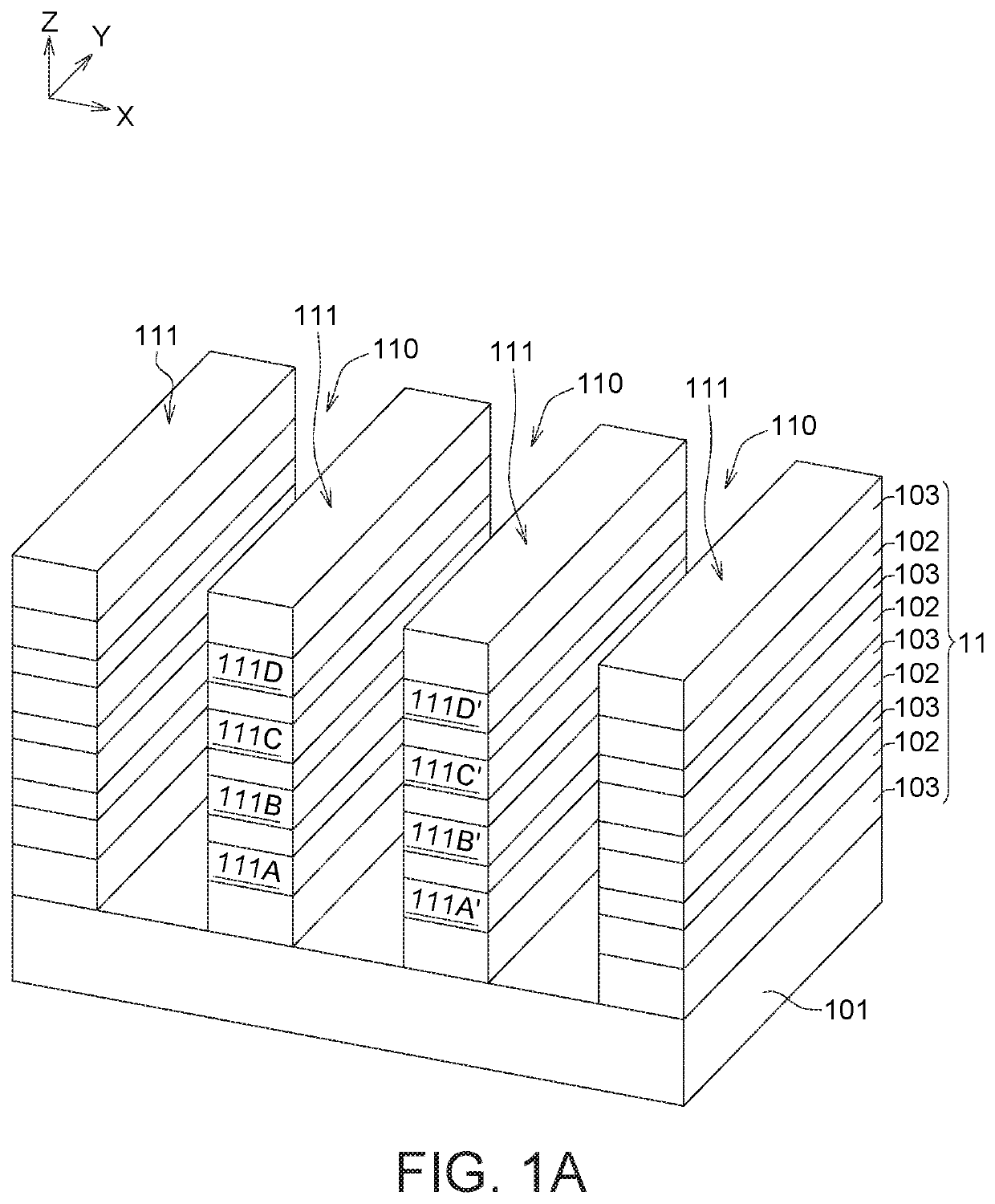
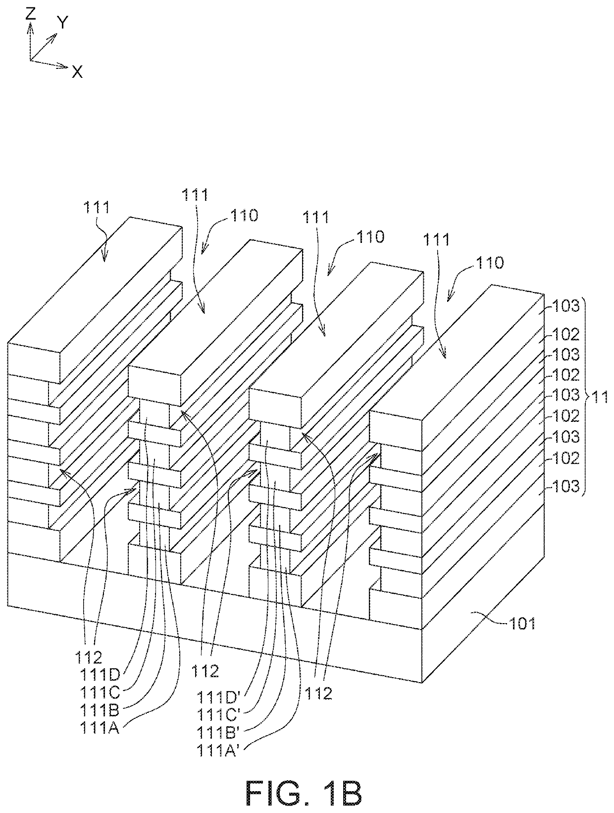
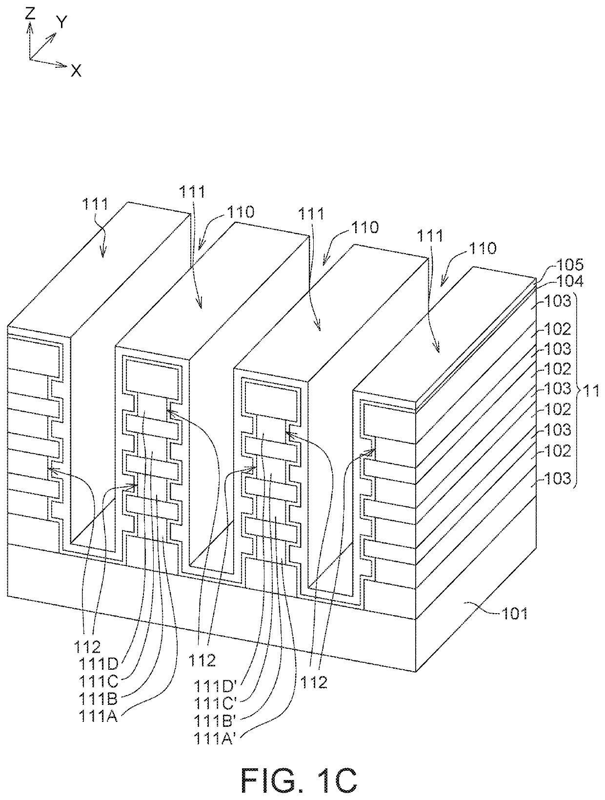
[0018]The embodiments as illustrated below provide a 3D memory device, the method for fabricating the same and applications thereof to perform sum-of-products operations. The present disclosure will now be described more specifically with reference to the following embodiments illustrating the structure and arrangements thereof.

[0019]It is to be noted that the following descriptions of preferred embodiments of this disclosure are presented herein for purpose of illustration and description only. It is not intended to be exhaustive or to be limited to the precise form disclosed. Also, it is also important to point out that there may be other features, elements, steps and parameters for implementing the embodiments of the present disclosure which are not specifically illustrated. Thus, the specification and the drawings are to be regard as an illustrative sense rather than a restrictive sense. Various modifications and similar arrangements may be provided by the persons skilled in the...


PUM

PropertyMeasurementUnit
programming currentaaaaaaaaaa
bias voltagesaaaaaaaaaa

Abstract

A 3D memory device includes a multi-layers stacking structure having a plurality of conductive layers and insulating layers stacked in a staggered manner, at least one trench passing through the conductive layers and a plurality of recess regions extending into the conductive layers from the trench; a dielectric blocking strip lining sidewalls of the trench and the recess regions; a plurality of floating gates disposed in the recess regions and isolated from the conductive layers by the dielectric blocking strip; a dielectric strip overlies sidewalls of the floating gates exposed from the recess regions; a semiconductor strip disposed in the trench, insulated from the floating gates by the dielectric strip, and includes a first doping region, a second doping region and a channel region disposed between and connects to the first doping region and the second doping region, and overlapping with the floating gates.

Description

BACKGROUNDTechnical Field[0001]The disclosure in generally relates to a memory device, fabricating method and applications thereof, and more particularly to a high-density three dimensional (3D) memory device, the fabricating method thereof, and applying the same for execution of a sum-of-products operation.Description of the Related Art[0002]In neuromorphic computing systems, machine learning systems and circuitry used for some types of computation based on linear algebra, the sum-of-products function can be an important component. The function can be expressed as follows:[0003]f⁡(xi)=∑i=1M⁢Wi⁢xi[0004]In this expression, each product term is a product of a variable input Xi and a weight Wi. The weight Wi can vary among the terms, corresponding for example to coefficients of the variable inputs Xi.[0005]The sum-of-products function can be realized as a circuit operation using cross-point array architectures in which the electrical characteristics of cells of the array effectuate the...

Claims


Application Information

Patent Timeline
Patent Type & Authority Patents(United States)
IPC IPC(8): H01L27/115H01L21/762H01L21/3213H01L21/28H01L21/311H01L21/02H01L27/11521H01L27/11526H01L27/11556H01L27/11568H01L27/11551H10B69/00H10B41/20H10B41/27H10B41/30H10B41/40H10B43/30
CPCH01L21/76224H01L21/32137H01L21/31116H01L29/40114H01L27/11521H01L21/02595H01L27/11556H01L21/02636H01L21/02532H01L27/11526H01L21/76227H01L21/76232H01L27/11568H01L27/11551G11C16/0408H10B41/10H10B41/50H10B41/20H10B41/27H10B41/30H10B41/40H10B43/30
Inventor LUE, HANG-TINGCHEN, WEI-CHEN
Owner MACRONIX INT CO LTD
Features
  • R&D
  • Intellectual Property
  • Life Sciences
  • Materials
  • Tech Scout
  • Unparalleled Data Quality
  • Higher Quality Content
  • 60% Fewer Hallucinations
Learn More