
Method for calculating pixel voltage for liquid crystal on silicon display device

a liquid crystal display device and liquid crystal technology, applied in static indicating devices, instruments, non-linear optics, etc., can solve the problems of degrading display performance, generating fringing field effects, and relatively expensive dlp display devices

Active Publication Date: 2020-09-15
HIMAX DISPLAY INC
View PDF37 Cites 3 Cited by
  • Summary
  • Abstract
  • Description
  • Claims
  • Application Information

AI Technical Summary

Benefits of technology

The invention provides a liquid crystal on silicon display device and a method for calculating a pixel voltage. The device includes a silicon substrate and a color filter layer with multiple sub-pixels. The sub-pixels have a pixel electrode and a common electrode. The color filter layer has multiple color filter units that correspond to the sub-pixels. The method involves obtaining multiple grey levels of a pixel and transforming them into multiple color values. For each sub-pixel, a parameter of a reflectance fitting function is obtained and a gamma correction is performed to obtain a reflectance. The reflectance is then used to calculate the pixel voltage, which is applied to the pixel electrode of the corresponding sub-pixel. The technical effects of the invention include improved display quality and reduced power consumption.

Problems solved by technology

However, LCD display devices have disadvantages of dead pixels and screen door effect, which degrades display performance.
However, DLP display devices are relatively expensive.
However, sub-pixels in the LCOS display device are close to each other, and thus a fringing field effect may be generated.
It is an issue to those skilled in the art about hot to address the fringing field effect.

Method used


Image

  • Method for calculating pixel voltage for liquid crystal on silicon display device
  • Method for calculating pixel voltage for liquid crystal on silicon display device
  • Method for calculating pixel voltage for liquid crystal on silicon display device

Examples


Embodiment Construction

[0026]Specific embodiments of the present invention are further described in detail below with reference to the accompanying drawings, however, the embodiments described are not intended to limit the present invention and it is not intended for the description of operation to limit the order of implementation. Moreover, any device with equivalent functions that is produced from a structure formed by a recombination of elements shall fall within the scope of the present invention. Additionally, the drawings are only illustrative and are not drawn to actual size.

[0027]The using of “first”, “second”, “third”, etc. in the specification should be understood for identifying units or data described by the same terminology, but are not referred to particular order or sequence.

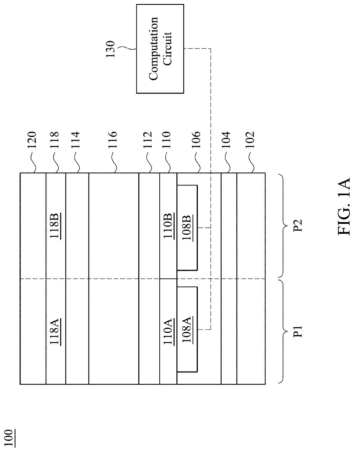
[0028]FIG. 1A is a local cross-sectional view of a LCOS display device 100 in accordance with an embodiment. The LCOS display device 100 includes a silicon substrate 102, a reflective layer 104, a dielectric layer 106,...


PUM

PropertyMeasurementUnit
reflectance fittingaaaaaaaaaa
reflectanceaaaaaaaaaa
voltageaaaaaaaaaa

Abstract

A liquid crystal on silicon display device is provided. Multiple grey levels of a pixel are transformed into multiple color values. The grey levels respectively correspond to multiple first sub-pixels. For each of the first sub-pixels, at least one parameter of a reflectance fitting function is obtained according to the color values, a gamma correction is performed according to the corresponding grey level to obtain a reflectance, and a pixel voltage is calculated according to the at least one parameter and the reflectance. The pixel voltage is applied to a pixel electrode of the corresponding first sub-pixel.

Description

BACKGROUNDField of Invention[0001]The present invention relates to a method for calculating a pixel voltage of a liquid crystal on silicon display device.Description of Related Art[0002]Nowadays, various kinds of projective display devices, such as liquid crystal display (LCD) display devices, digital light processing (DLP) display devices and liquid crystal on silicon (LCOS) display devices, are commercially available. Among these display devices, the LCD display devices operate in a transmissive way, while the DLP display devices and the LCOS display devices operate in a reflective way. LCD display devices are the oldest and the most popular, and have advantages such as high color accuracy and low manufacture cost. However, LCD display devices have disadvantages of dead pixels and screen door effect, which degrades display performance. DLP display devices have advantages such as high contrast ratio and immune to color decay. However, DLP display devices are relatively expensive. L...

Claims


Application Information

Patent Timeline
Patent Type & Authority Patents(United States)
IPC IPC(8): G02F1/13G09G3/36G02F1/1362
CPCG02F1/136277G09G3/3607G09G3/3696G09G2320/0673G02F2203/30G02F2201/121G02F2201/123G02F2001/136222G02F1/136222
Inventor LI, YUET-WINGCHEN, WEN-HSU
Owner HIMAX DISPLAY INC
Learn More