Light emitting diode panel and manufacturing method thereof

a technology of light-emitting diodes and manufacturing methods, applied in semiconductor/solid-state device testing/measurement, identification means, instruments, etc., can solve problems such as invalidation, failure to successfully transfer, damage to micro-light-emitting diodes transferred to the substrate, etc., to ensure the yield of light-emitting diodes and improve repair efficiency

Active Publication Date: 2021-10-12
AU OPTRONICS CORP
View PDF13 Cites 0 Cited by
  • Summary
  • Abstract
  • Description
  • Claims
  • Application Information

AI Technical Summary

Benefits of technology

[0008]Based on the above, apart from the first light emitting diodes predetermined to display images, the light emitting diode panel in accordance with the embodiment of the invention further includes the second light emitting diode for repair. In addition, the configuration region of the second light emitting diode is surrounded by the configuration regions of a plurality of first light emitting diodes. When the first light emitting diode predetermined to display images is detected as invalid, a repair method is to electrically connect the second light emitting diode to the corresponding control signal line of the invalid first light emitting diode, so that the second light emitting diode replaces the invalid first light emitting diode to display images. As such, the yield of the light emitting diode panel is ensured. Besides, any one of the plurality of first light emitting diodes disposed in the first regions surrounding the second light emitting diode may be repaired by using the second light emitting diode to achieve a better repair efficiency.

Problems solved by technology

Since the micro light emitting diode is not easy to be tested individually, and it is not easy to bond a single micro light emitting diode to the substrate independently, the micro light emitting diodes are mostly batch transferred to the substrate.
Accordingly, some of the micro light emitting diodes transferred to the substrate may be damaged, invalid, or not successfully transferred.

Method used


Image

  • Light emitting diode panel and manufacturing method thereof
  • Light emitting diode panel and manufacturing method thereof
  • Light emitting diode panel and manufacturing method thereof

Examples


Embodiment Construction

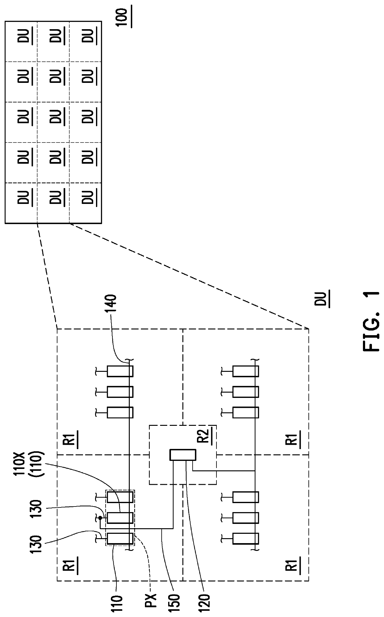
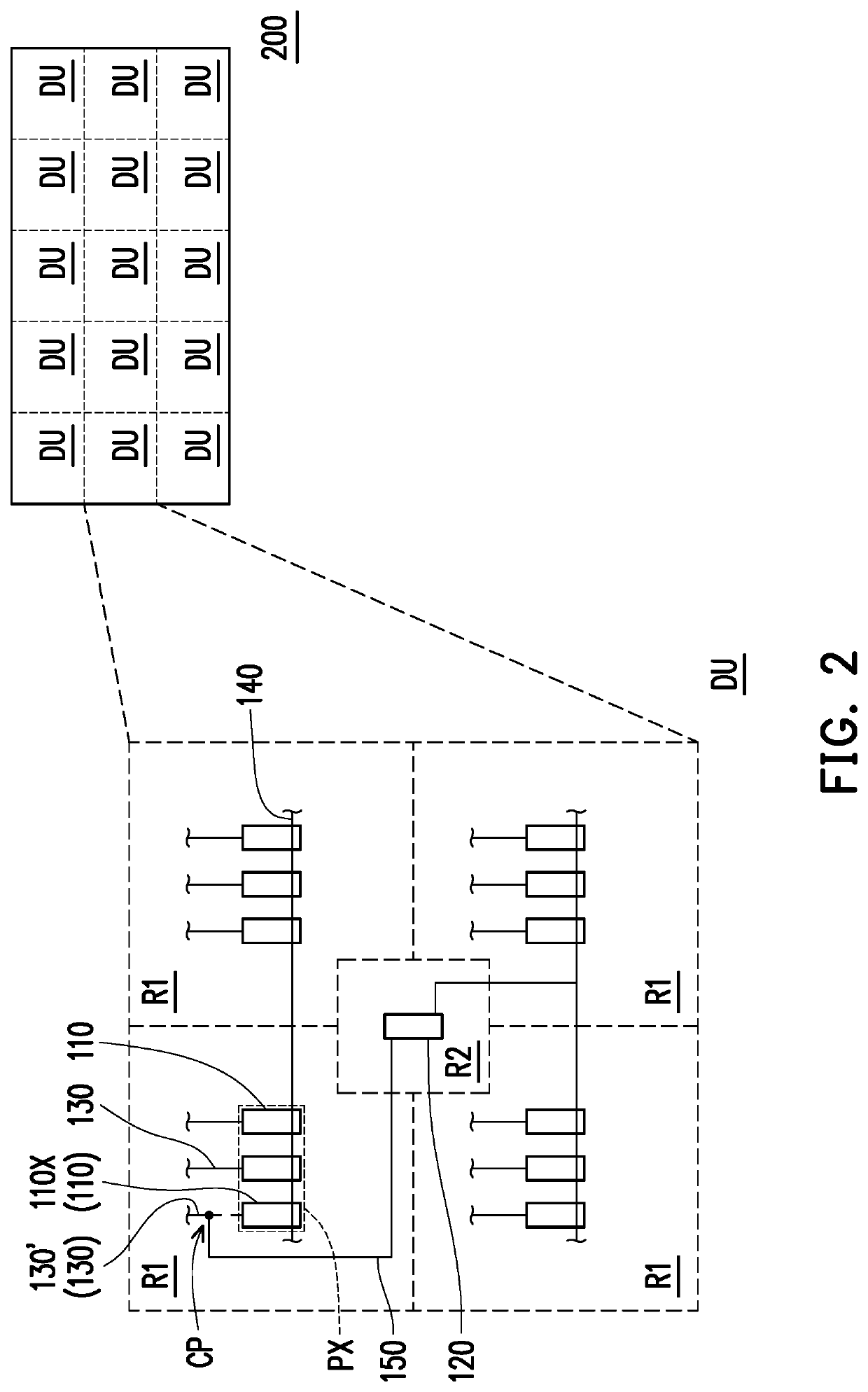
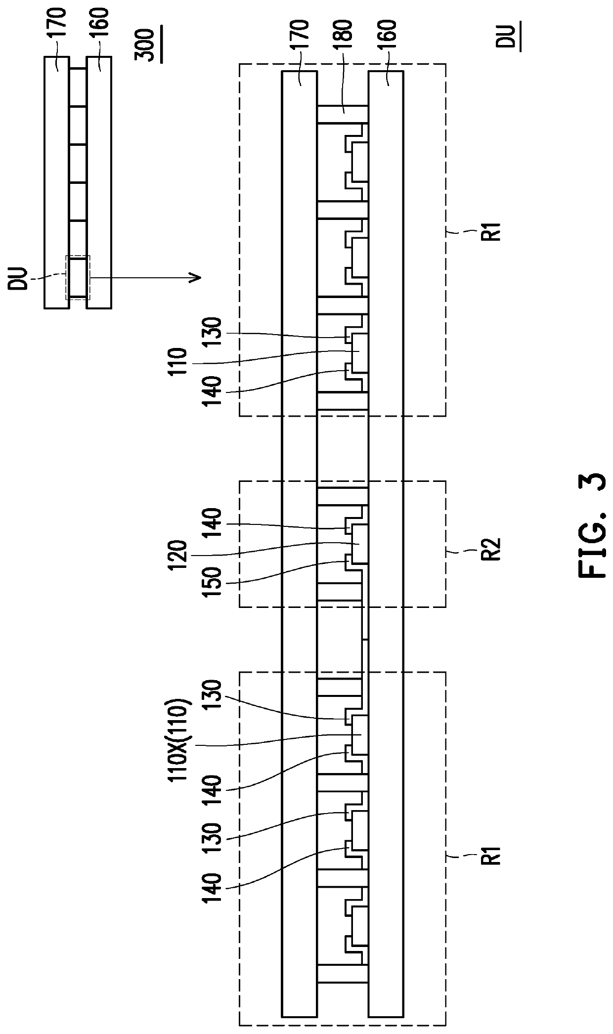
[0027]FIG. 1 is a schematic diagram illustrating a top-view of a micro light emitting diode panel according to an embodiment of the invention. Please refer to FIG. 1. A light emitting diode panel 100 includes a plurality of display units DU. The plurality of display units DU are arranged in an array manner in the top-view. In addition, the display unit DU may be distributed throughout on the light emitting diode panel 100, and there is unnecessary to keep a border. However, the embodiment is not limited thereto. It may be acquired from a partial enlarged view of the display unit DU of FIG. 1 that a single display unit DU may include a plurality of first light emitting diodes 110 and a second light emitting diode 120. Specifically, each display unit DU is divided into a plurality of first regions R1 and a second region R2 surrounded by the plurality of first regions R1 according to the arrangement of the first light emitting diodes 110 and the second light emitting diode 120.

[0028]Ev...


PUM

PropertyMeasurementUnit
side lengthaaaaaaaaaa
lengthaaaaaaaaaa
luminous efficiencyaaaaaaaaaa

Abstract

A light emitting diode panel including a first substrate, a second substrate and a plurality of display units is provided. The display units are disposed between the first substrate and the second substrate. One display unit has multiple first regions and a second region surrounded by the first regions and includes multiple first light emitting diodes, multiple control signal lines and a second light emitting diode. Every N first light emitting diodes construct one pixel unit located within one of the first regions, wherein N is an integer greater than 1. The control signal lines are disposed on the first substrate and each extends toward one first light emitting diode. The second light emitting diode is disposed on the first substrate, located within the second region, and surrounded by the first regions. The second light emitting diode is electrically connected to one of the control signal lines.

Description

CROSS-REFERENCE TO RELATED APPLICATION[0001]This application claims the priority benefit of Taiwan application serial no. 108105698, filed on Feb. 20, 2019. The entirety of the above-mentioned patent application is hereby incorporated by reference herein and made a part of this specification.BACKGROUND OF THE INVENTIONField of the Invention[0002]The invention relates to an electronic device, and in particular, to a light emitting diode panel.Description of Related Art[0003]Light emitting diodes have functions such as high luminous efficiency, power saving, and good reliability, and have been widely applied to various fields. In the application of a display, a technology of a display panel applied a micro light emitting diode as a display structure has been further developed. Regarding the manufacturing method of the micro light emitting diode panel, the manufactured micro light emitting diode array is bonded to the substrate by a batch transfer process, and the process is completed ...

Claims


Application Information

Patent Timeline
Patent Type & Authority Patents(United States)
IPC IPC(8): H01L27/15H01L25/075H01L21/66H01L33/50H01L33/62
CPCH01L25/0753H01L22/20H01L33/505H01L33/62H01L2933/0041H01L2933/0066H01L27/156G09F9/33H01L33/50H01L33/0095
Inventor LO, KUO-LUNGLIU, PIN-MIAOCHEN, JHAO-WUNWU, TSUNG-TIEN
Owner AU OPTRONICS CORP
Why Eureka
Try Eureka