
Active discharge circuitry for display matrix

a technology of active discharge circuitry and display matrix, which is applied in the direction of static indicating devices, electrical appliances, instruments, etc., can solve the problems of time-multiplexing display system, side effects such as ghosting, spike noise, or phantom noise, and unwanted lighting emission, so as to facilitate discharge activities, reduce ghosting effects, and accelerate charge discharg

Active Publication Date: 2021-11-09
PLANAR SYSTEMS
View PDF13 Cites 0 Cited by
  • Summary
  • Abstract
  • Description
  • Claims
  • Application Information

AI Technical Summary

Benefits of technology

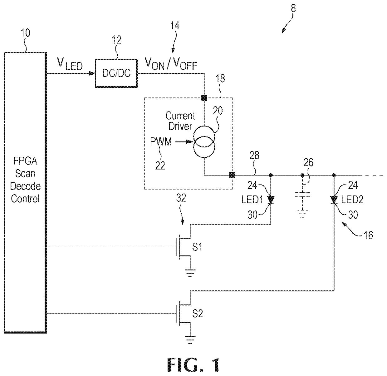
[0007]Active discharge circuitry for rapid discharging of charge on an LED display matrix includes a mechanism to effectuate electrically connecting a charged node to a discharge circuit for controlled discharge of any unwanted charge. In some embodiments, a discharge path is provided for discharging the node until it reaches a desired (e.g., programmable) value. The active discharge circuitry includes a control circuit generating appropriate timing and digital control signals for starting and stopping (i.e., actuating) a switch facilitating the discharge activities. The disclosed techniques accommodate variations in channel-to-channel start times for mitigating ghosting effects that would otherwise be presented by the LED display matrix due to residual (i.e., unwanted) charges remaining electrically loaded on display elements (LEDs) via, for example, charged parasitic capacitance or other such transients, after a current driver of a specific channel has stopped driving the display elements.
[0008]According to one embodiment, ghosting effects are reduced by discharging a charge stored by parasitic capacitance coupled to a channel of an LED display. Specifically, circuity receives a timing signal indicating that the charge is available to be discharged for at least a portion of a time following a PWM cycle and preceding a new scan cycle. In response to the timing signal, the circuity compares a reference voltage signal with a discharge voltage signal attributable to the charge. The circuitry applies to a switch device an actuation signal that, based on the comparing, actuates the switch device and thereby couples the channel to a discharge path.
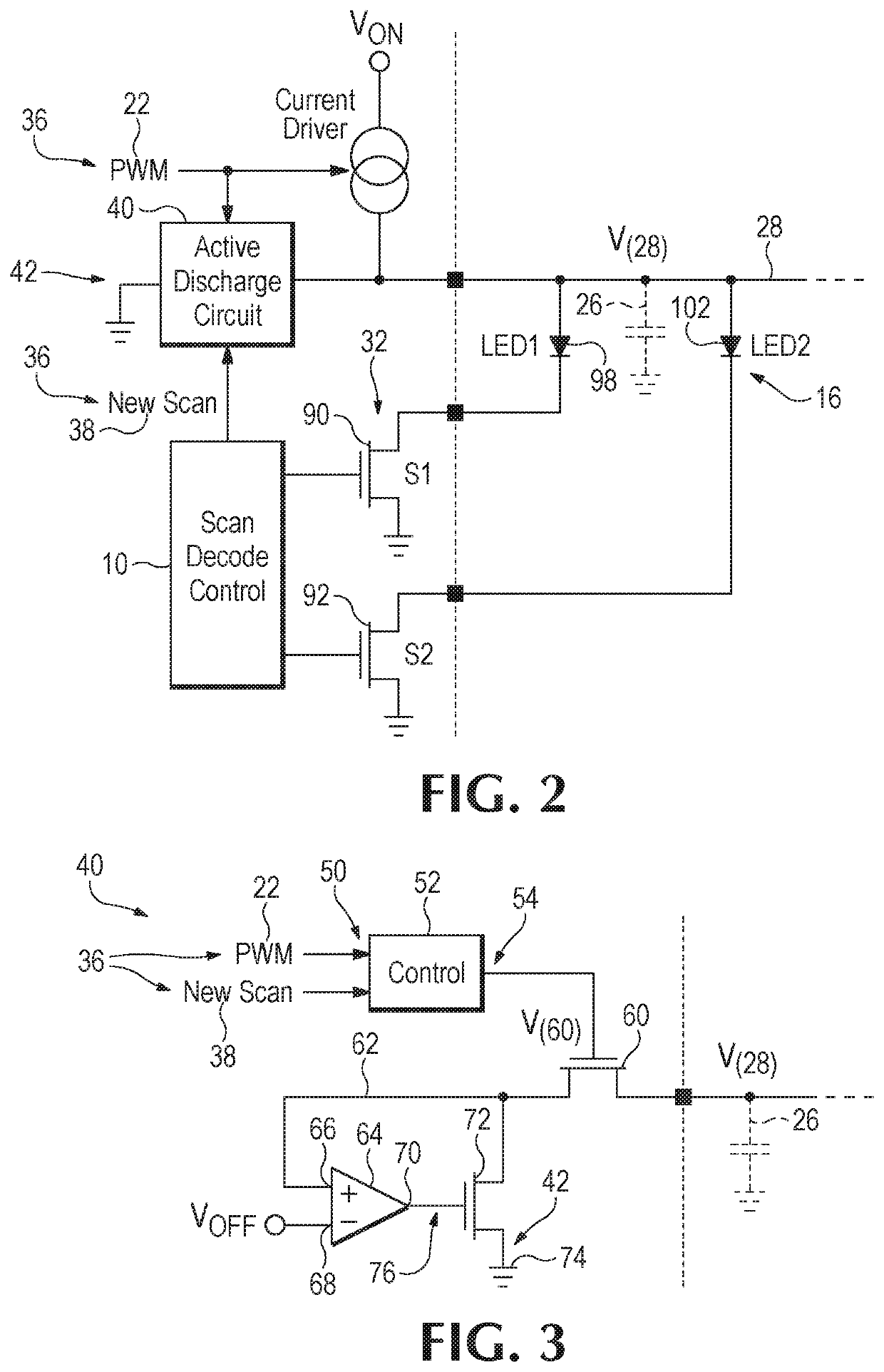
[0009]In another embodiment, active discharge circuitry reduces ghosting effects by controlling discharge of a charge stored by parasitic capacitance coupled to a channel of a light-emitting diode (LED) display. The active discharge circuitry includes a comparator having first and second comparator inputs to which are applied, respectively, a discharge voltage signal attributable to the charge and a reference voltage signal, the comparator having a comparator output; a node on which the discharge voltage signal is provided; a first switch device having first, second, and third terminals coupled to, respectively, the node, the comparator output, and a discharge path; and a second switch device that, in response to application of an active discharge control signal, is actuated to cause the comparator to compare the discharge voltage signal applied to the first comparator input and the reference voltage signal applied to the second comparator input so as to generate at the comparator output a comparison signal applied to the second terminal of the first switch device that, based on the comparison signal, controllably couples the channel to the discharge path.

Problems solved by technology

One drawback of time-multiplexing display systems is a side-effect called ghosting, spike noise, or phantom noise, which are typically perceived as unwanted lighting emission.

Method used


Image

  • Active discharge circuitry for display matrix
  • Active discharge circuitry for display matrix
  • Active discharge circuitry for display matrix

Examples


first embodiment

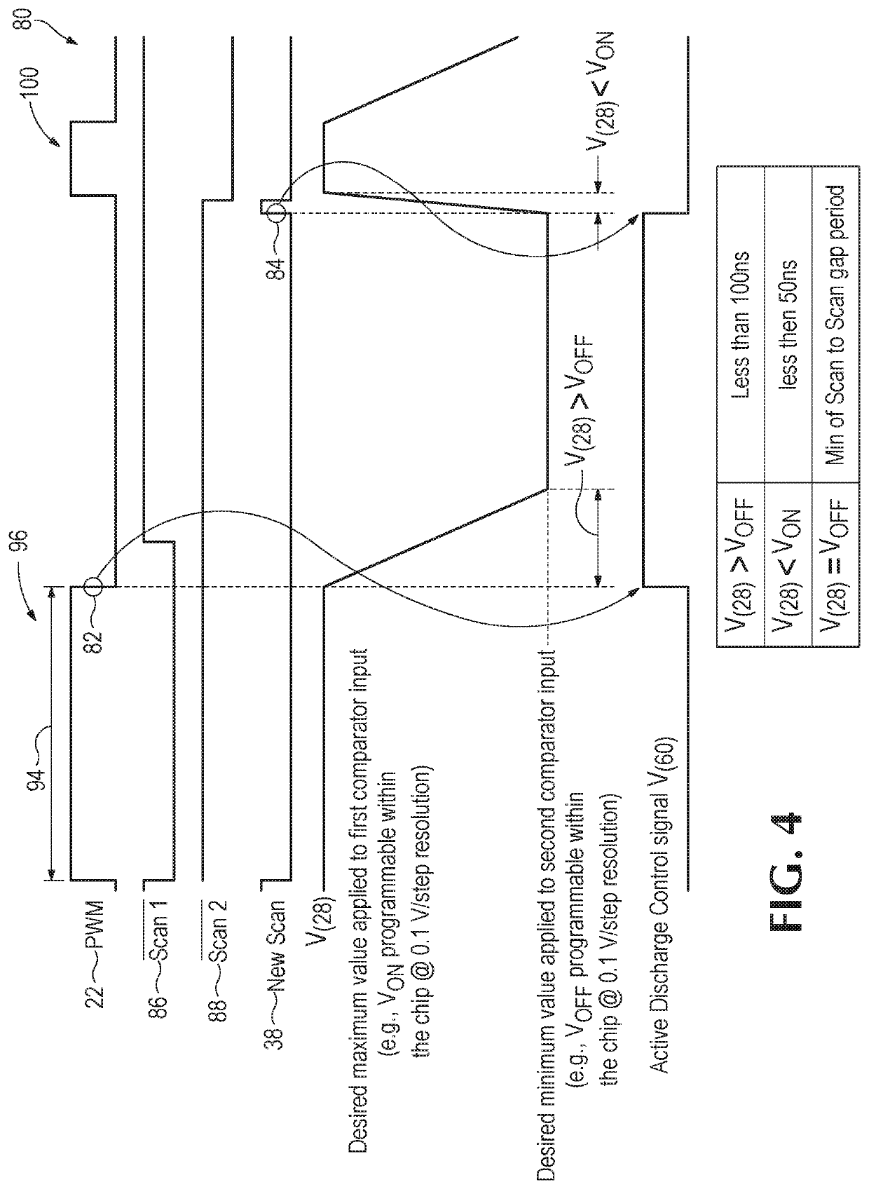
[0026]FIG. 4 is a timing diagram 80 showing signal timing for performing active ghost elimination according to a For channel 28 shown in FIGS. 2 and 3, as a trailing edge 82 (falling edge) of PWM signal 22 is detected by active discharge control logic 52 (FIG. 3), active discharge control logic 52 changes a state (i.e., from low to high) of active discharge control signal V(60). Active discharge control signal V(60) is then applied by controller output 54 to the gate of switch 60 (FIG. 3), which is thereby actuated to start the active discharge operation described previously. The operation may then end after a specific clock-counting period (or other predetermined discharge time), or it may end at a leading edge 84 of a new scan cycle indicated by new scan signal 38. Skilled persons will appreciate that a similar sequence and circuitry may also be implemented for other channels in a multi-channel system.

[0027]For completeness, also shown in FIG. 4 are a first scan signal 86 and a s...

second embodiment

[0028]FIG. 5 is a timing diagram 110 showing signal timing for performing active ghost elimination according to a In this embodiment, new scan signal 38 initiates and stops the active discharge operation. A new scan signal is typically generated as a single grayscale clock (GCLK) pulse wherein the leading edge occurs one clock pulse width before the completion of the current scan and the trailing edge is synchronized with the completion of the current scan. Additional description of an example of a GCLK and its relationship with PWM and scan timing is available in International Application Publication No. WO 2018 / 098036 titled “Intensity Scaled Dithering Pulse Width Modulation,” of Nadershahi.

[0029]The described features, operations, or characteristics may be arranged and designed in a wide variety of different configurations or combined in any suitable manner in one or more embodiments. Thus, the detailed description of the embodiments of the systems and methods is not intended to...


PUM


Abstract

Active discharge circuitry for fast discharging of charge on an LED display matrix includes a mechanism to effectuate circuit path switching so as to electrically connect a charged node to a discharge circuit for controlled discharging of unwanted charge until it reaches a desired (e.g., programmable) value. The active discharge circuitry includes a control circuit generating appropriate timing and digital control signals for starting and stopping (e.g., actuating a switch) the discharge activities. The disclosed techniques accommodate variations in channel-to-channel start times for mitigating ghosting effects that would otherwise be presented from the LED display matrix due to residual (i.e., unwanted) charges remaining electrically loaded on display elements via, for example, charged parasitic capacitance or other such transients, after a current driver of a specific channel has stopped driving.

Description

RELATED APPLICATIONS[0001]This application is a National Stage of International Application No. PCT / US2018 / 062656, filed Nov. 27, 2018, which claims priority benefit of U.S. Provisional Patent Application No. 62 / 592,375, filed Nov. 29, 2017, which are hereby incorporated by reference in their entireties.TECHNICAL FIELD[0002]This disclosure generally relates to light-emitting diode (LED) drivers and, more particularly, to ghost image prevention for an LED-matrix driver.BACKGROUND INFORMATION[0003]An LED display panel generally refers to a device which comprises an array of LEDs that are arranged in one or more rows and columns. An LED display panel may include a plurality of sub-modules, each sub-module having one or more such LED arrays. LED display panels may employ arrays of LEDs of a single color or different colors. When LEDs of the same color are used in certain display applications, each LED normally corresponds to a display unit or pixel. When LED panels employ LEDs of differ...

Claims


Application Information

Patent Timeline
Patent Type & Authority Patents(United States)
IPC IPC(8): G09G3/20G09G3/32H03K7/08H05B45/46G09G3/36
CPCG09G3/32G09G2310/0267G09G2320/04G09G2310/0251G09G3/2014
Inventor NADERSHAHI, SHAHNAD
Owner PLANAR SYSTEMS
Learn More