Method and electronic device for controlling data communication

a technology of electronic devices and data communication, applied in the direction of electric digital data processing, instruments, computing, etc., can solve the problems of affecting and reducing the communication speed of electronic devices. , to achieve the effect of stable high-speed communication, reducing the communication speed of electronic devices, and improving the stability of high-speed communication

Active Publication Date: 2022-02-01
SAMSUNG ELECTRONICS CO LTD
View PDF29 Cites 2 Cited by
  • Summary
  • Abstract
  • Description
  • Claims
  • Application Information

AI Technical Summary

Benefits of technology

[0005]In a wireless communication environment, an electronic device may have a limitation to data transmission according to a used communication scheme. For example, a Wi-Fi communication has a disadvantage that a communication speed of the electronic device may be decreased due to interference, and that the greater the number of other electronic devices which ac

Problems solved by technology

In a wireless communication environment, an electronic device may have a limitation to data transmission according to a used communication scheme.
For example, a Wi-Fi communication has a disadvantage that a communication speed of the electronic device may be decreased due to interference, and that the greater the number of other electronic devices which acces

Method used


Image

  • Method and electronic device for controlling data communication
  • Method and electronic device for controlling data communication
  • Method and electronic device for controlling data communication

Examples


Embodiment Construction

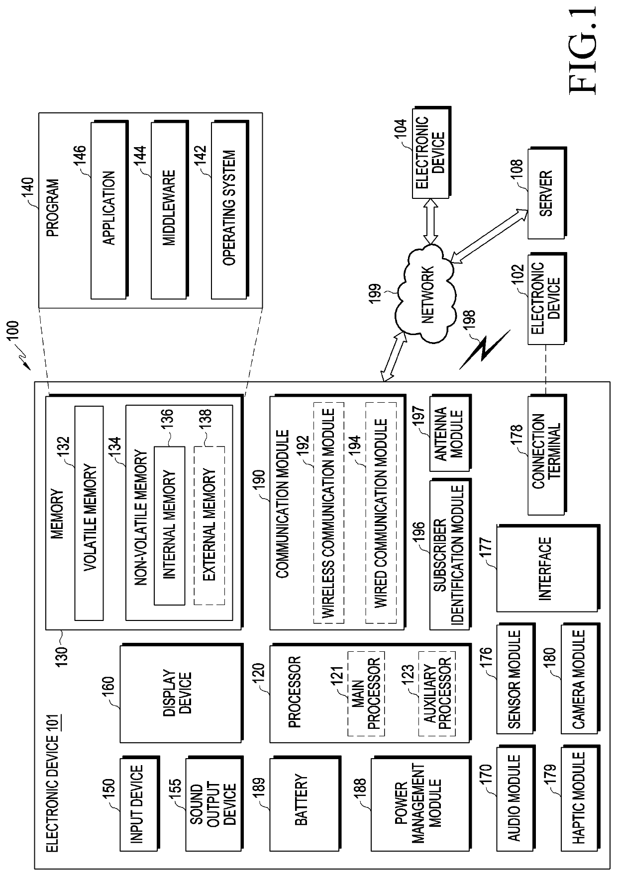
[0032]FIG. 1 is a block diagram illustrating an electronic device 101 in a network environment 100 according to various embodiments. Referring to FIG. 1, the electronic device 101 in the network environment 100 may communicate with an electronic device 102 via a first network 198 (e.g., a short-range wireless communication network), or an electronic device 104 or a server 108 via a second network 199 (e.g., a long-range wireless communication network). According to an embodiment, the electronic device 101 may communicate with the electronic device 104 via the server 108. According to an embodiment, the electronic device 101 may include a processor 120, a memory 130, an input device 150, a sound output device 155, a display device 160, an audio module 170, a sensor module 176, an interface 177, a haptic module 179, a camera module 180, a power management module 188, a battery 189, a communication module 190, a subscriber identification module (SIM) 196, or an antenna module 197. In s...


PUM


Abstract

The electronic device according to various embodiments comprises: a housing structure; a user interface located in the housing structure; a network interface that can be connected by wire or wirelessly; a wireless communication circuit configured to communicate with an external device by using frequencies between 10 GHz and 100 GHz; a processor located in the housing structure and operatively connected to the user interface, the network interface, and the wireless communication circuit; and a memory located in the housing structure and operatively connected to the processor. When the memory is running, the processor may: establish a first communication channel with a first external device by means of the wireless communication circuit; receive authentication information from the first external device by means of the first communication channel; receive data from the first external device by means of the first communication channel, while or after receiving the authentication information; store the received data in the memory at least temporarily; establish a second communication channel with a second external device by means of the network interface, by using the authentication information; and store commands for transmitting the stored data to the second external device by means of the second communication channel. Other embodiments are possible.

Description

CROSS-REFERENCE TO RELATED APPLICATION(S)[0001]This application is a National Phase Entry of PCT international Application No. PCT / KR2019 / 000519, which was filed on Jan. 14, 2019, and claims priority to Korean Patent Application No. 10-2018-0007349 filed on Jan. 19, 2018 in the Korean Intellectual Property Office, the contents of which are incorporated herein by reference.BACKGROUND1. Field[0002]Various embodiments relate to a method and electronic device to control a data communication.2. Description of the Related Art[0003]With development of wireless communication technologies, a data transmission speed has been improved. In addition, various electronic devices using wireless communication technologies have been developed.[0004]Recently, a standard for an ultra-high speed wireless transmission technology using a millimeter wave has been developed. The millimeter wave system may generally mean a system using an ultra-high frequency of 30 to 300 GHz. For example, a WiGig communicat...

Claims


Application Information

Patent Timeline
IPC IPC(8): H04W12/06
CPCH04W12/06G06F3/041H04L63/0853H04W4/80H04L63/0428H04L67/1097H04L63/18H04L63/08H04L67/06
Inventor LEE, JUNGHUNNAM, CHOUNJONGKANG, DOOSUKLEE, SUNKEYCHOI, BOKUN
Owner SAMSUNG ELECTRONICS CO LTD
Why Eureka
Try Eureka