
Resistive random access memory structure and manufacturing method thereof

a random access and memory structure technology, applied in the field of memory devices, can solve the problems of difficult control of the electrical resistance value of the low-resistance state, large operating voltage, and different size of the conductive filaments produced in the transition, so as to improve the yield and reliability of the final product, the effect of improving the stability of the device and the variable operating voltag

Active Publication Date: 2022-02-22
WINBOND ELECTRONICS CORP
View PDF8 Cites 0 Cited by
  • Summary
  • Abstract
  • Description
  • Claims
  • Application Information

AI Technical Summary

Benefits of technology

[0007]The disclosure provides a RRAM structure and a manufacturing method thereof. By using this manufacturing method, the positions where the conductive filaments are formed can be precisely controlled. Therefore, the variability of the operating voltage and the stability of the device can be improved, thereby improving the yield and reliability of the final product.
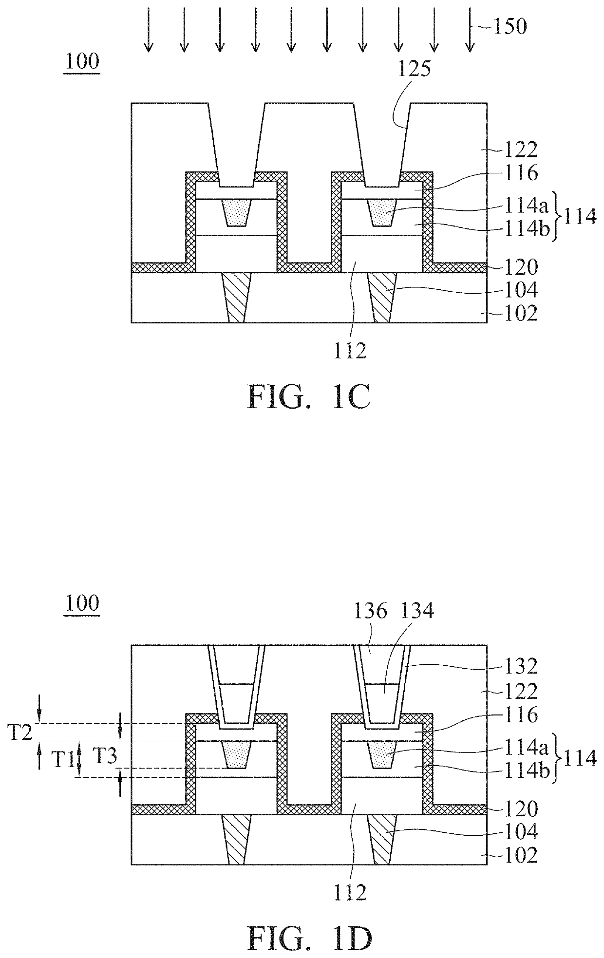
[0010]In the RRAM structure provided by the embodiments of the present invention, most of the conductive filaments con be confined in a specific region (i.e., the conductive filament confined region). Therefore, the variability of the operating voltage and the stability of the device can be improved. Furthermore, in the manufacturing method of the RRAM structure provided by the present invention, the top electrode is formed by filling the conductive material into the opening located directly above the conductive filament confined region. Therefore, the undercut does not occur on the sidewall of the top electrode layer, and the yield and reliability of the final product can be further improved.

Problems solved by technology

Therefore, the position and size of the conductive filaments that are produced in the transitions are different and uncontrollable.
In other words, it is difficult to control the electrical resistance value of the low-resistance state.
As a result, the variability in the operating voltage is large and the stability of the device is poor, such that the yield and reliability of the final product are reduced.

Method used


Image

  • Resistive random access memory structure and manufacturing method thereof
  • Resistive random access memory structure and manufacturing method thereof
  • Resistive random access memory structure and manufacturing method thereof

Examples


Embodiment Construction

[0015]The present disclosure is best understood from the following detailed description when read with the accompanying figures. It should be noted that, in accordance with the standard practice in the industry, various features are not drawn to scale. In fact, the relative dimensions of the various features may be arbitrarily increased or reduced for clarity of discussion. In addition, the present disclosure may repeat reference numerals and / or letters in the various examples. This repetition is for the purpose of simplicity and clarity and does not in itself dictate a relationship between the various embodiments and / or configurations discussed.

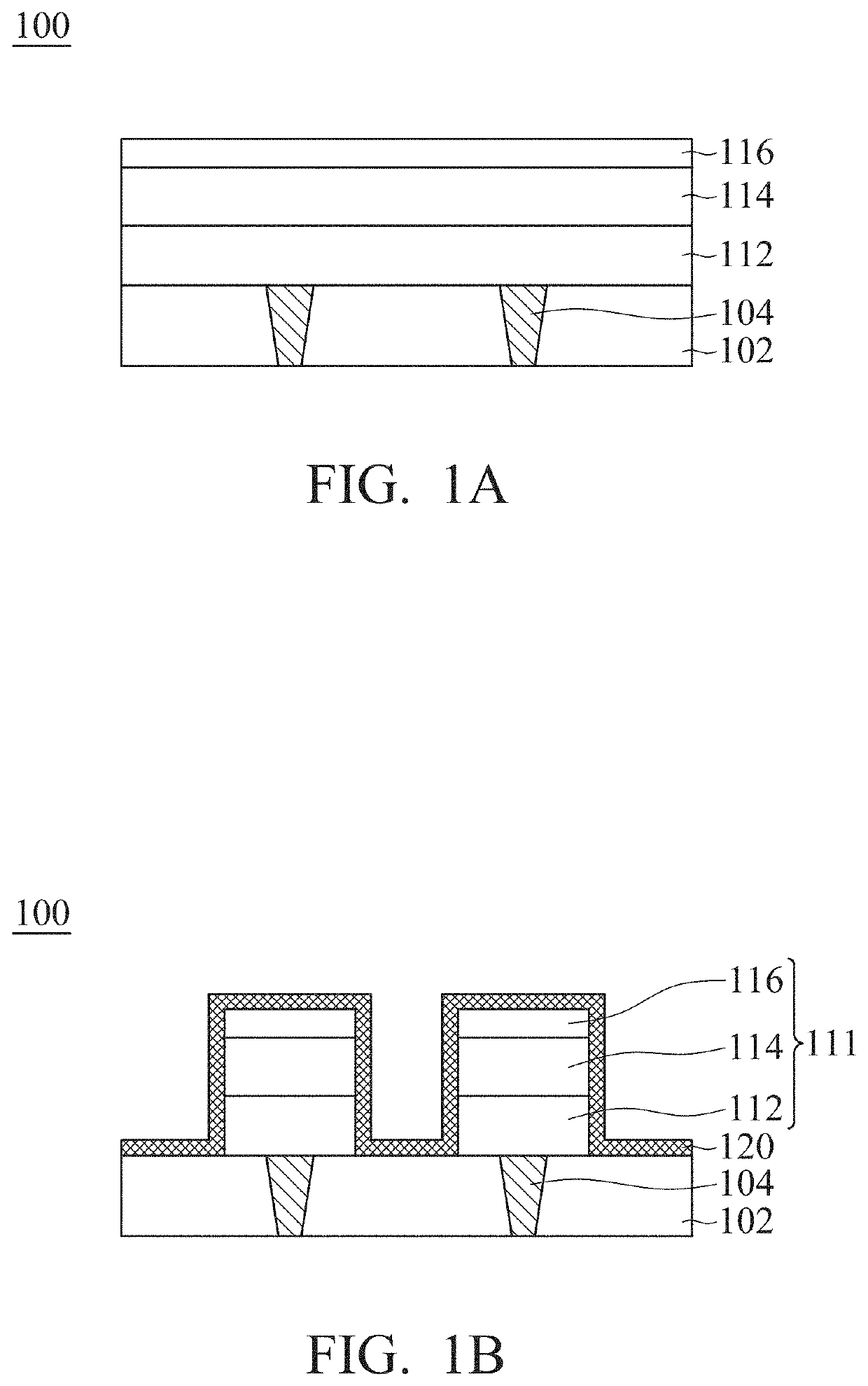
[0016]FIGS. 1A-1D show cross-sectional views of various stages of forming a RRAM structure 100 in accordance with some embodiments of the present invention. Referring to FIG. 1A, a substrate 102 is provided. The material of the substrate 102 may include a bulk semiconductor substrate (for example, a silicon substrate), a compound semiconduct...


PUM

PropertyMeasurementUnit
energyaaaaaaaaaa
thicknessaaaaaaaaaa
resistanceaaaaaaaaaa

Abstract

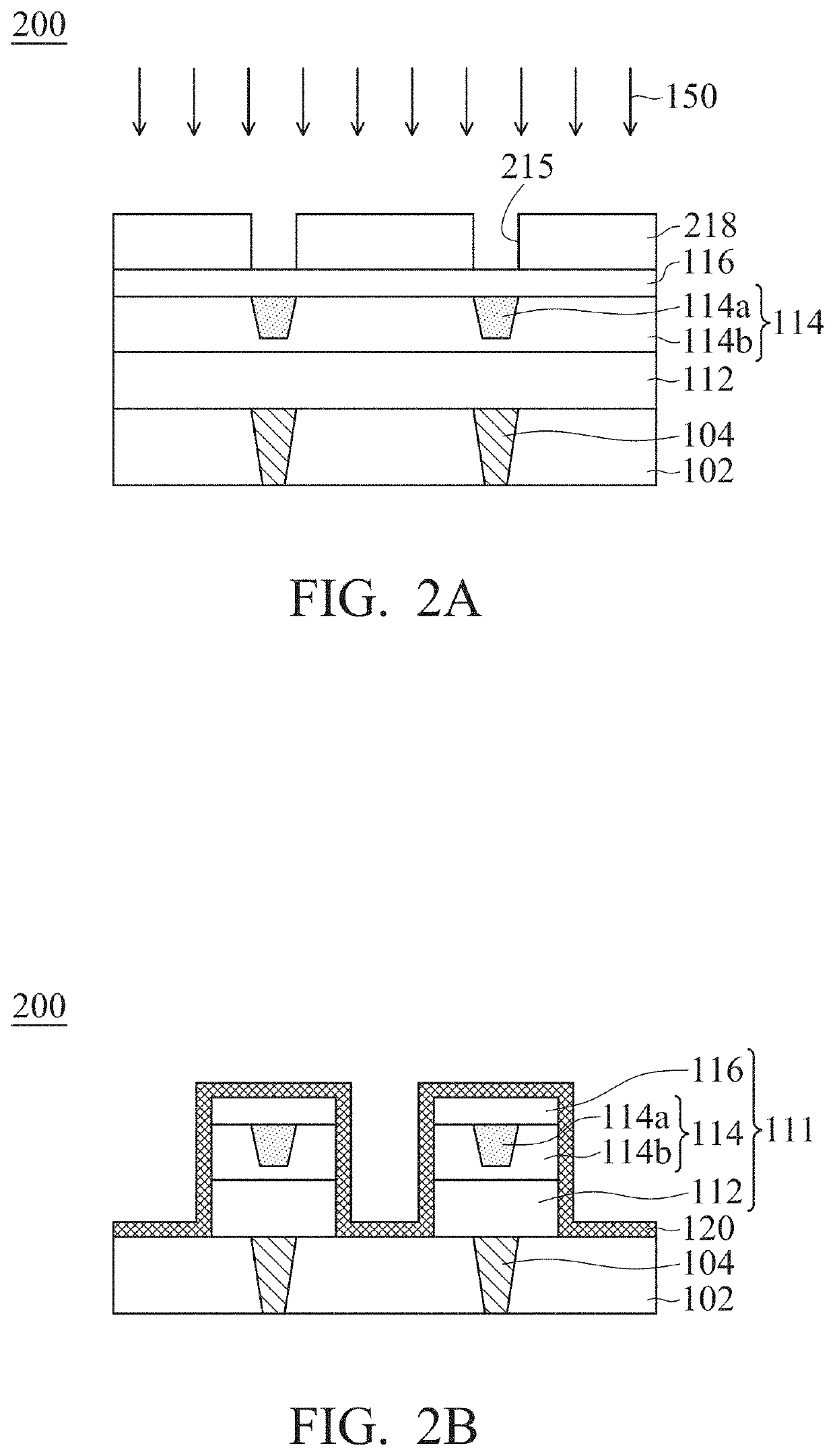
An RRAM structure and its manufacturing method are provided. The RRAM structure includes a bottom electrode layer, a resistance switching layer, and an implantation control layer sequentially formed on a substrate. The resistance switching layer includes a conductive filament confined region and an outer region surrounding the conductive filament confined region. The RRAM structure includes a protective layer and a top electrode layer. The protective layer conformally covers the bottom electrode layer, the resistance switching layer, and the implantation control layer and has a first opening. The top electrode layer is located on the implantation control layer, and a portion of the top electrode layer is filled into the first opening. The position of the top electrode layer corresponds to that of the conductive filament confined region, and the top surface of the top electrode layer is higher than that of the protective layer.

Description

CROSS REFERENCE TO RELATED APPLICATIONS[0001]This Application claims priority of Taiwan Patent Application No. 108123070, filed on Jul. 1, 2019, the entirety of which is incorporated by reference herein.BACKGROUNDField of the Disclosure[0002]The present disclosure relates to a memory device, and in particular it relates to a resistive random access memory structure and a method for manufacturing the resistive random access memory structure.Description of the Related Art[0003]Resistive random access memory (RRAM) has several advantages, such as its simple structure, small area, low operating voltage, fast operating speed, long memory time, capability for multi-bit storage, and low power consumption. Hence, RRAM has great potential to replace the current flash memory for being the main non-volatile memory used in the next generation.[0004]When a forming voltage or a writing voltage is applied to a RRAM structure, oxygen ions are driven by the voltage and move away from the resistance ...

Claims


Application Information

Patent Timeline
Patent Type & Authority Patents(United States)
IPC IPC(8): H01L45/00H01L27/24
CPCH01L45/165H01L27/2463H01L45/08H01L45/1253H01L45/146H01L45/1658H01L45/1233H10N70/24H10N70/826H10N70/841H10N70/8833H10N70/043H10B63/80H10N70/046
Inventor WU, BO-LUNHSU, PO-YENSHEN, TING-YINGLIN, MENG-HUNG
Owner WINBOND ELECTRONICS CORP
Learn More