
Method, apparatus, and system for global healing of stability-limited die through bias temperature instability

a technology of temperature instability and stability limitation, applied in the field of manufacturing and using sophisticated semiconductor devices, can solve the problems of reducing the yield of circuit elements more than, and bti tending to weaken the drive strength of transistors, etc., to achieve the effect of improving the yield and/or reliability of semiconductor devices

Inactive Publication Date: 2017-03-21
GLOBALFOUNDRIES INC
View PDF1 Cites 0 Cited by
  • Summary
  • Abstract
  • Description
  • Claims
  • Application Information

AI Technical Summary

Benefits of technology

This patent is about a method of improving the yield and reliability of semiconductor devices using a process called bias temperature instability (BTI). The method involves measuring the stability and writing failures of a group of cells in an array. By comparing the number of stability failures and writing failures, the method identifies a ratio that indicates the stability of a cell. If this ratio is high, meaning the cell has low stability, a higher write voltage is applied to the pass gate of each cell for a short duration to improve reliability. Overall, this method can increase the yield and reliability of semiconductor devices.

Problems solved by technology

Over time, BTI tends to weaken the drive strength of the transistor.
Of further concern in multi-element devices, such as, for example, six-transistor (6T) SRAMs, is that unequal extents of BTI between different elements may lead to imbalances between writeability and read-stability (one cause of which is BTI shifts) that reduce yield of the circuit element more than would be expected from simply considering each BTI-undergoing element in isolation.
Field failures due to stress induced device shifts attributable to the BTI mechanism continue to plague very-large-scale integration (VLSI) CMOS technologies.
Over product life time the Vmin is known to increase in large SRAM arrays due to negative bias temperature instability (NBTI) and more recently positive bias temperature instability (PBTI) combined with NBTI.
SRAM arrays are particularly vulnerable due to the increased number of bits with each generation and use of minimum transistor size for maximum bit density.
The random nature of the BTI mechanism leaves large arrays vulnerable to BTI induced failures over the life time of the product.
Therefore, BTI induced voltage sensitive failures in advanced VLSI SRAM arrays are expected to remain one of the key technology reliability concerns for the foreseeable future.
Though accepted, voltage-guard-bands are costly with limitations in effectiveness.

Method used


Image

  • Method, apparatus, and system for global healing of stability-limited die through bias temperature instability
  • Method, apparatus, and system for global healing of stability-limited die through bias temperature instability
  • Method, apparatus, and system for global healing of stability-limited die through bias temperature instability

Examples


example

[0043]Although the next several paragraphs will discuss an example of healing of bits with failing stability, the person of ordinary skill in the art, having the benefit of the present disclosure, will understand the applicability of the example to the healing of bits with failing writeability.

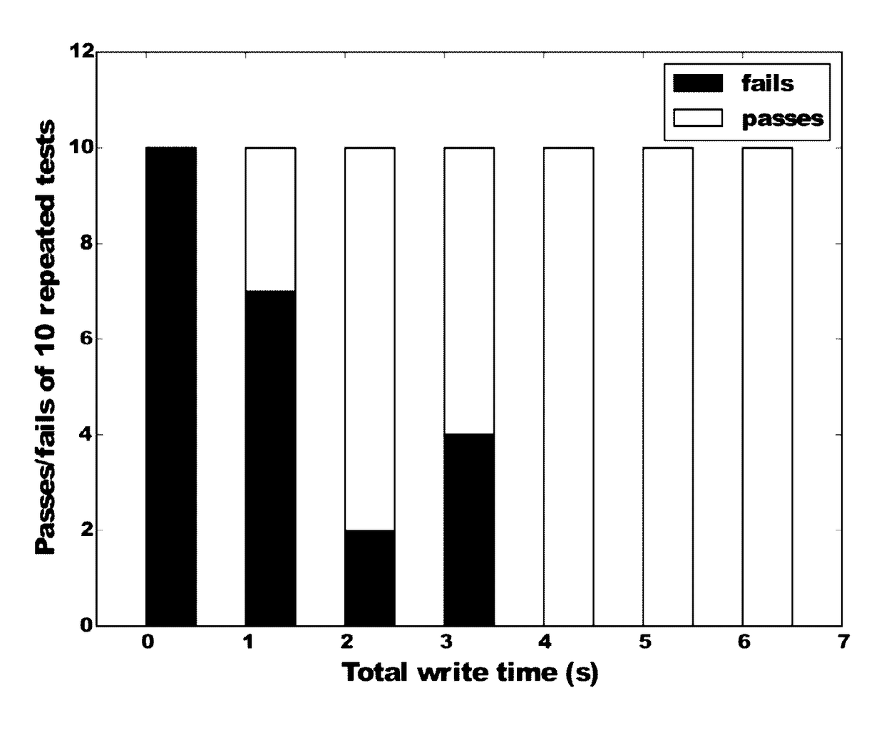
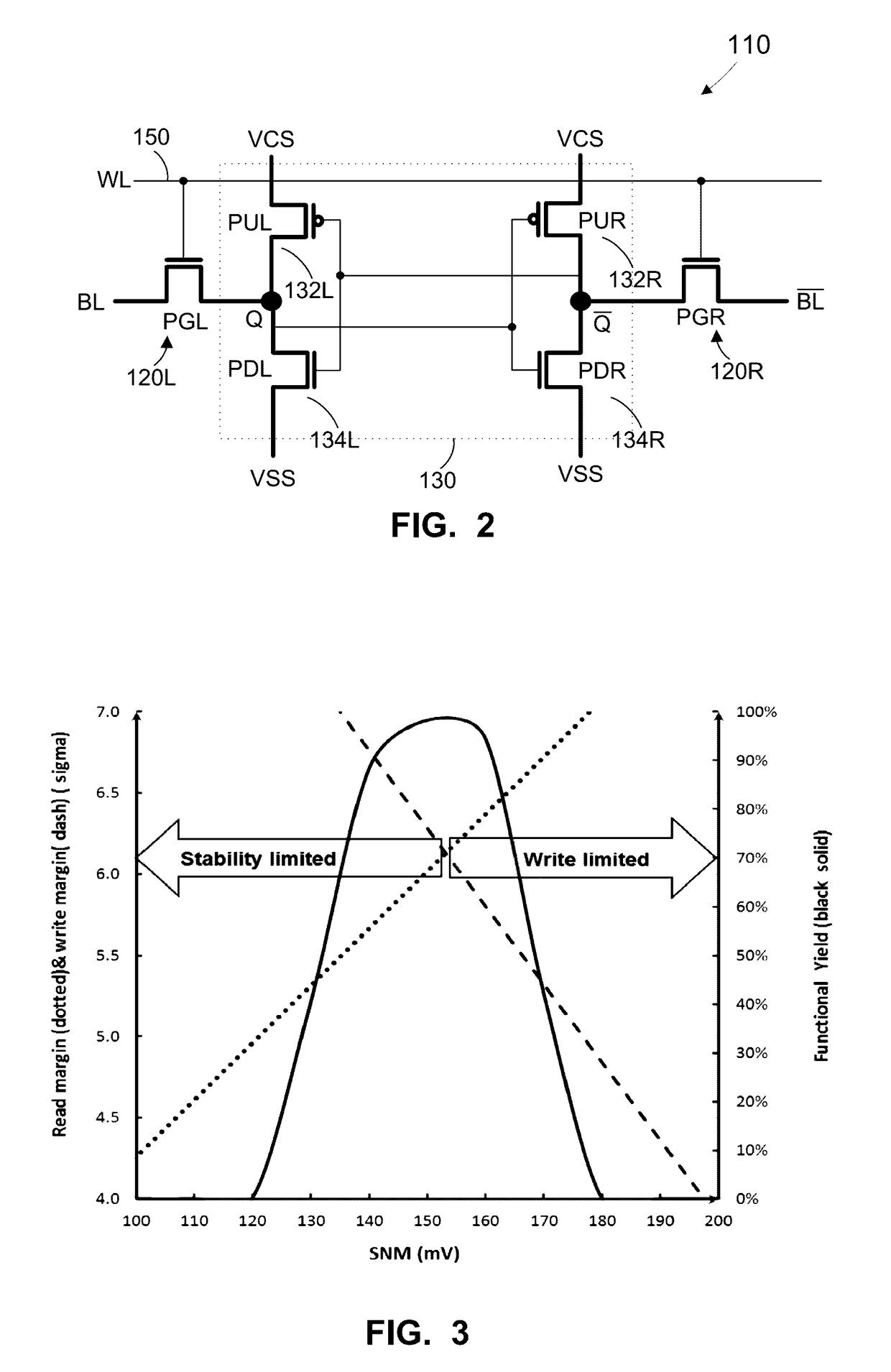
[0044]Though not to be bound by theory, turning to FIGS. 3-7, we review how to significantly reduce the vulnerability to BTI fails. By controlled selective bias of targeted failing bits, fails or shifts in Vmin can be rectified. This is accomplished with existing array design architectures using only the existing built in terminals (BL, BL, WL, VCS and VSS).

[0045]The concepts required for “healing” of failed or failing bits in large SRAM arrays on advanced CMOS nodes are discussed and demonstrated with both (20 nm and 14 nm) hardware. As scaling continues below 20 nm, greater than 500 Mb of SRAM on a die is not uncommon. The migration to FinFET devices and the lithographic challenges in printi...


PUM


Abstract

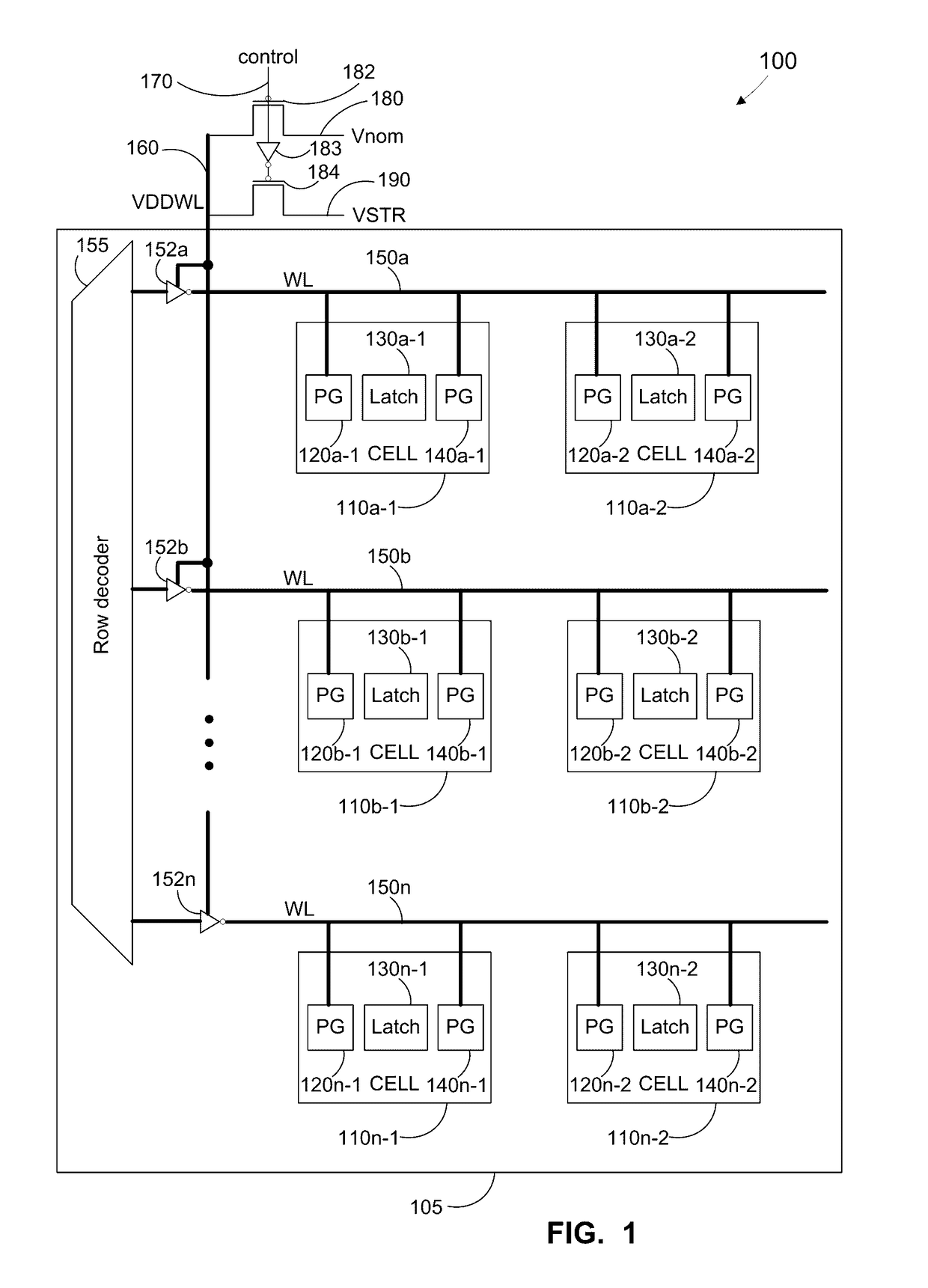
We disclose methods, apparatus, and systems for improving semiconductor device yield and / or reliability through bias temperature instability (BTI). One device may comprise a plurality of cells of an array, wherein each of the cells comprises a pass gate and a latch; a plurality of word lines, wherein each word line controls access to each pass gate of a first number of cells; a word line driver electrically connected to each word line; and a control line configured to provide an operational write voltage or a first write voltage to each word line through the word line driver. By virtue of BTI, application of the first write voltage may lead to improved stability of data desired to be read from one or more cells of the device.

Description

BACKGROUND OF THE INVENTION[0001]Field of the Invention[0002]Generally, the present disclosure relates to the manufacture and use of sophisticated semiconductor devices, and, more specifically, to various methods, structures, and systems for improving the yield and / or reliability of semiconductor devices by exploitation of bias temperature instability (BTI).[0003]Description of the Related Art[0004]The manufacture of semiconductor devices requires a number of discrete process steps to create a packaged semiconductor device from raw semiconductor material. The various processes, from the initial growth of the semiconductor material, the slicing of the semiconductor crystal into individual wafers, the fabrication stages (etching, doping, ion implanting, or the like), to the packaging and final testing of the completed device, are so different from one another and specialized that the processes may be performed in different manufacturing locations that contain different control schemes...

Claims


Application Information

Patent Timeline
Patent Type & Authority Patents(United States)
IPC IPC(8): G11C11/00G11C11/419G11C7/06
CPCG11C11/419G11C7/065G11C7/04G11C8/08G11C11/418G11C29/56
Inventor GAUTAM, AKHILESHMANN, RANDY W.MCMAHON, WILLIAMRANDRIAMIHAJA, YOANN MAMYSONG, YUNCHENG
Owner GLOBALFOUNDRIES INC
Learn More