Method of manufacturing semiconductor device

a manufacturing method and semiconductor technology, applied in semiconductor devices, semiconductor/solid-state device details, electrical devices, etc., can solve the problems of unavoidable loss or thinning of cap film 8 during etching, and achieve the effects of high yield, reduced capacity, and increased reliability

Active Publication Date: 2008-12-04
PANNOVA SEMIC
View PDF3 Cites 335 Cited by
  • Summary
  • Abstract
  • Description
  • Claims
  • Application Information

AI Technical Summary

Benefits of technology

[0021](3) The barrier properties against Si or 0 atoms in the interlayer insulating film 11.This disadvantageously reduces the yield and reliability of the semiconductor device.
[0022]The present invention is devised in view of these problems. An object of the present invention is to provide a method of manufacturing a semiconductor device which enables a sufficient reduction in the capacity between wires and which offers a high yield and increased reliability.

Problems solved by technology

However, the inventors have found that the conventional technique poses the following problems.
However, since the selection ratio of the cap film 8 to the interlayer insulating film 2 and the inter-wire insulating film 3 is finite, the cap film 8 is unavoidably thinned or lost during the etching.

Method used


Image

  • Method of manufacturing semiconductor device
  • Method of manufacturing semiconductor device
  • Method of manufacturing semiconductor device

Examples


first embodiment

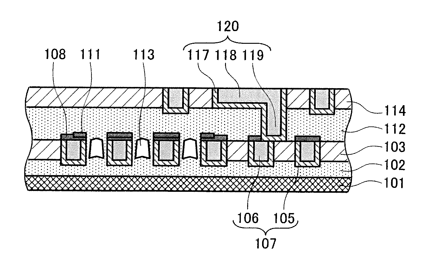
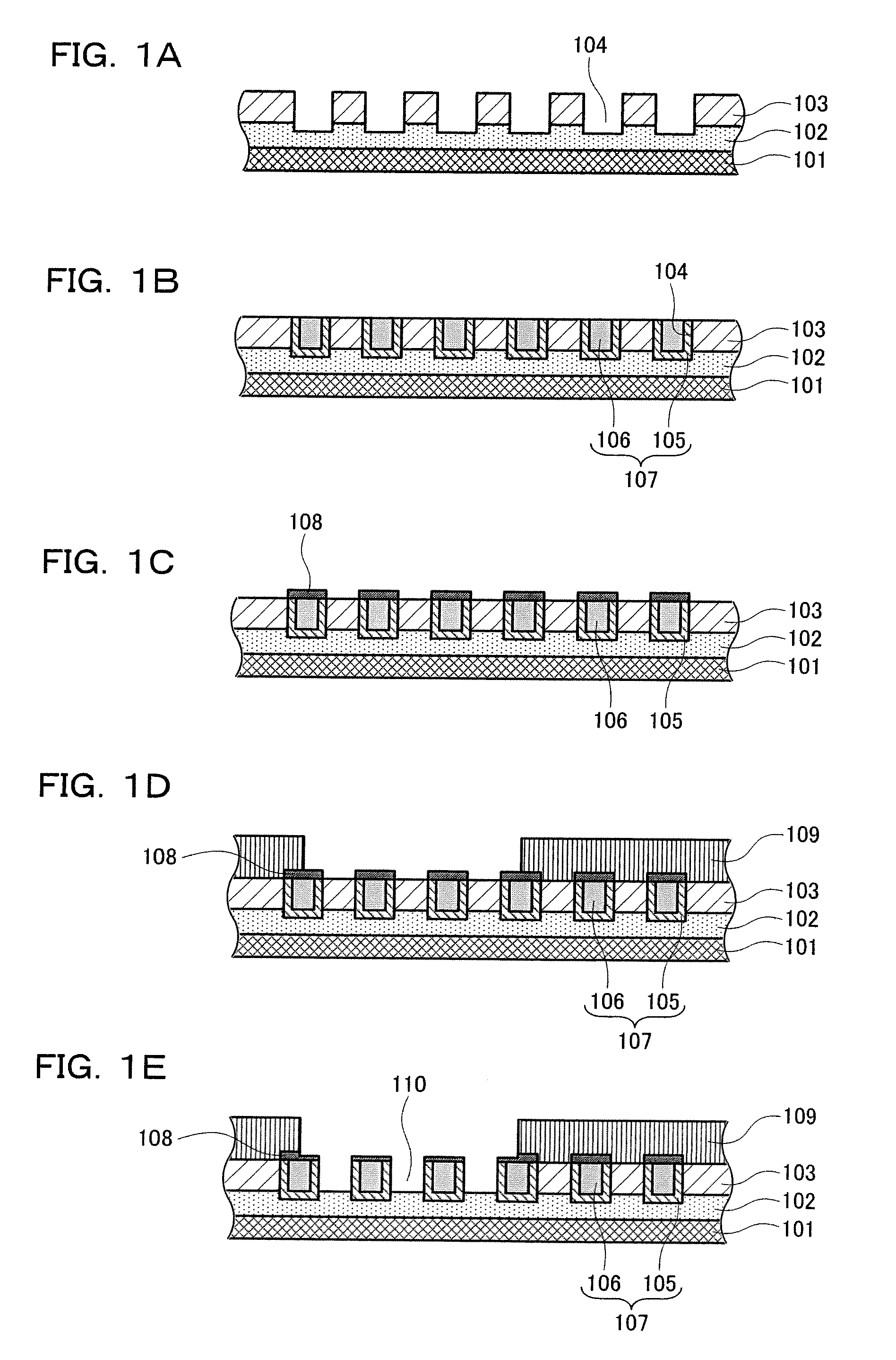
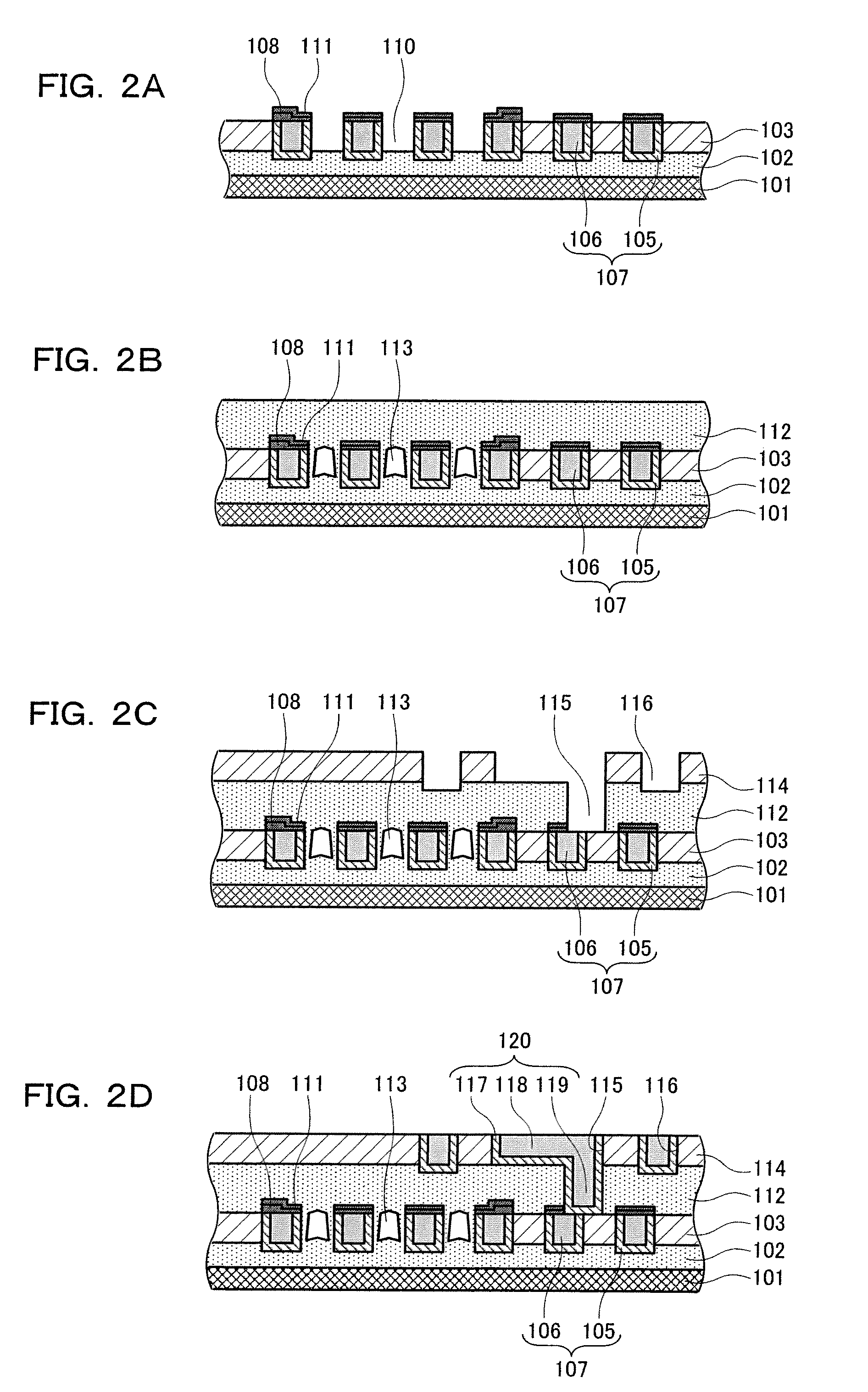
[0115]A first embodiment of the present invention will be described below with reference to FIGS. 1A, 1B, 1C, 1D, 1E, 2A, 2B, 2C, 2D, 3A, 3B, and 3C. FIGS. 1A, 1B, 1C, 1D, 1E, 2A, 2B, 2C, and 2D are sectional views illustrating steps of a method of manufacturing a semiconductor device according to the first embodiment. FIGS. 3A, 3B, and 3C are sectional views illustrating steps of the method of manufacturing the semiconductor device in which a second cap film is formed before a resist pattern is removed according to the first embodiment.

[0116]First, as shown in FIG. 1A, an interlayer insulating film 102 and an inter-wire insulating film 103 are deposited on a surface of a semiconductor substrate 101. Wiring grooves 104 are then formed in an upper part of a film stack of the interlayer insulating film 102 and the inter-wire insulating film 103 by photolithography and dry etching. In the present embodiment, an SiOC film is used as the interlayer insulating film 102, and an SiO2 film i...

second embodiment

[0150]A second embodiment of the present invention will be described below with reference to FIGS. 4A, 4B, 4C, 4D, 4E, 5A, 5B, 5C, 5D, 6A, 6B, and 6C. Only the differences of the present embodiment from the first embodiment will be described. The description of parts similar to those in the first embodiment is omitted.

[0151]FIGS. 4A, 4B, 4C, 4D, 4E, 5A, 5B, 5C, and 5D are sectional views illustrating steps of a method of manufacturing a semiconductor device according to the second embodiment. FIGS. 6A, 6B, and 6C are sectional views illustrating steps of the method of manufacturing the semiconductor device in which a second cap film is formed before a resist pattern is removed according to the second embodiment.

[0152]The present embodiment is different from the first embodiment in that a first cap film 108 has a fixed thickness of 10 nm in FIG. 5A. Thus, in FIG. 4E, when gaps 110 are each formed between lower wires 107, the first cap film 108 in an air gap forming area, which is not...

third embodiment

[0171]A third embodiment of the present invention will be described below with reference to FIGS. 7A, 7B, 7C, 7D, 7E, 8A, 8B, 8C, 8D, 9A, 9B, and 9C. Only the differences of the present embodiment from the first embodiment will be described. The description of parts similar to those in the first embodiment is omitted.

[0172]FIGS. 7A, 7B, 7C, 7D, 7E, 8A, 8B, 8C, 8D, 9A, 9B, and 9C are sectional views illustrating steps of a method of manufacturing a semiconductor device according to the third embodiment.

[0173]The present embodiment is different from the first embodiment in that a liner film 121 is deposited on surfaces of an inter-wire insulating film 103 and a first cap film 108 as shown in FIG. 7D.

[0174]First, as shown in FIG. 7A, an interlayer insulating film 102 and the inter-wire insulating film 103 are deposited on a surface of a semiconductor substrate 101. Wiring grooves 104 are then formed inside the layer stack of the interlayer insulating film 102 and the inter-wire insulat...


PUM


Abstract

A high-density N-type diffusion layer 116 formed in a separation area 115 makes it possible to reduce a collector current flowing through a parasitic NPN transistor 102. Thus, a normal CMOS process can be used to provide a driving circuit and a data line driver which make it possible to improve resistance to possible noise occurring between adjacent terminals, while controlling a chip size.

Description

FIELD OF THE INVENTION [0001]The present invention relates to a method of manufacturing a semiconductor device comprising an air gap structure that reduces capacity between wires.BACKGROUND OF THE INVENTION [0002]In recent years, miniaturization of semiconductor integrated circuit elements has reduced the intervals between elements and between wires internally connecting the elements together. This has disadvantageously increased the capacity between the wires to reduce a speed at which signals are propagated. Thus, examinations have been conducted of a method of forming an air gap between the wires to reduce the capacity. With reference to FIGS. 16A, 16B, 16C, 16D, 16E, 17A, 17B, 17C, and 17D, description will be given of a conventional method of manufacturing a semiconductor device having the air gap formed therein.[0003]FIGS. 16A, 16B, 16C, 16D, 16E, 17A, 17B, 17C, and 17D are sectional views illustrating steps of the conventional method of manufacturing the semiconductor device....

Claims


Application Information

Patent Timeline
Patent Type & Authority Applications(United States)
IPC IPC(8): H01L21/4763
CPCH01L21/7682H01L21/76832H01L21/76834H01L21/7685H01L21/76852H01L2924/0002H01L23/5222H01L2221/1078H01L2924/00H01L21/76849
Inventor HARADA, TAKESHISHIBATA, JUNICHIUEKI, AKIRA
Owner PANNOVA SEMIC
Why Eureka
Try Eureka