

Semiconductor device
- Summary
- Abstract
- Description
- Claims
- Application Information
AI Technical Summary
Benefits of technology
Problems solved by technology
Method used
Image

Examples
first embodiment
[First Embodiment]
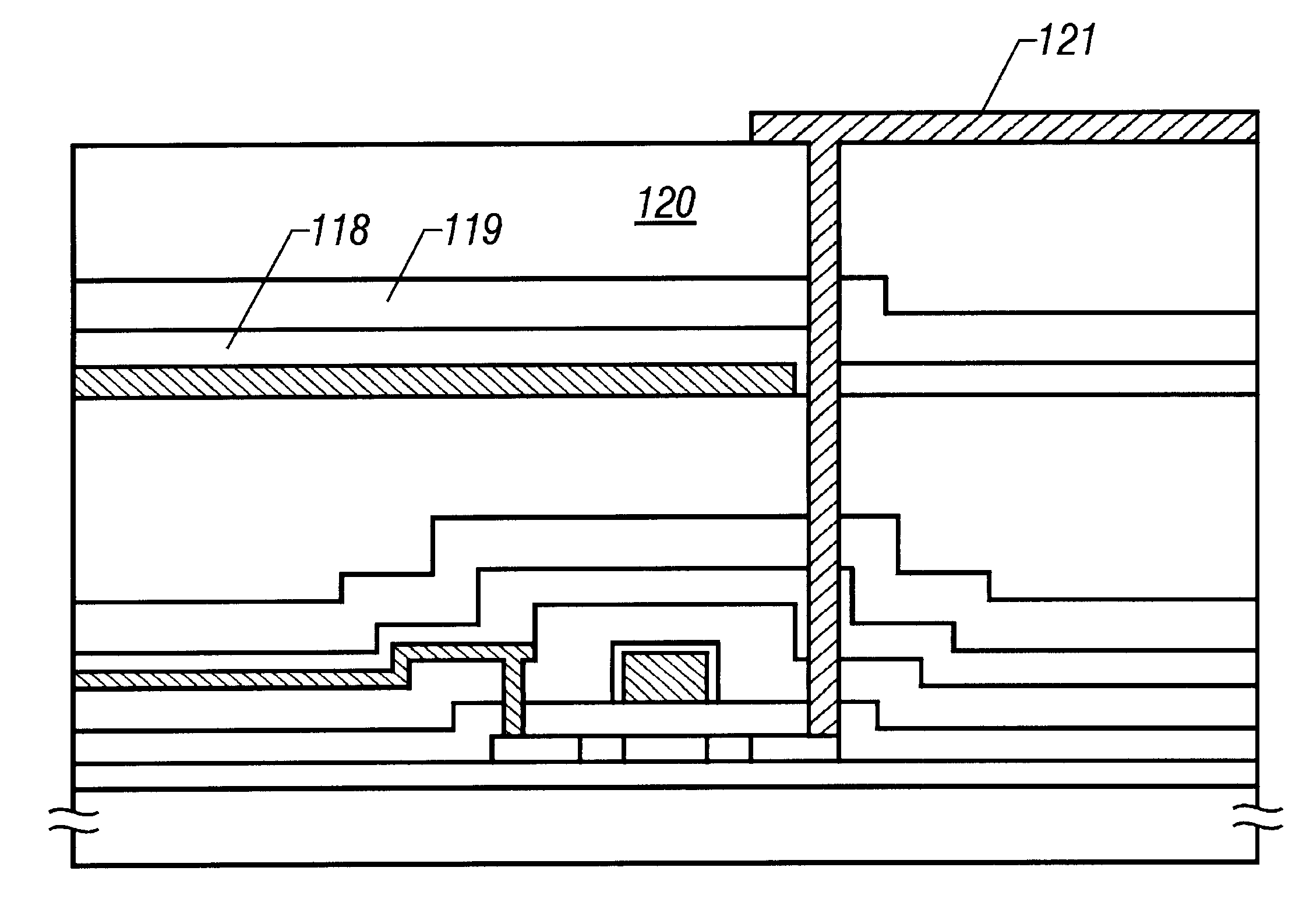
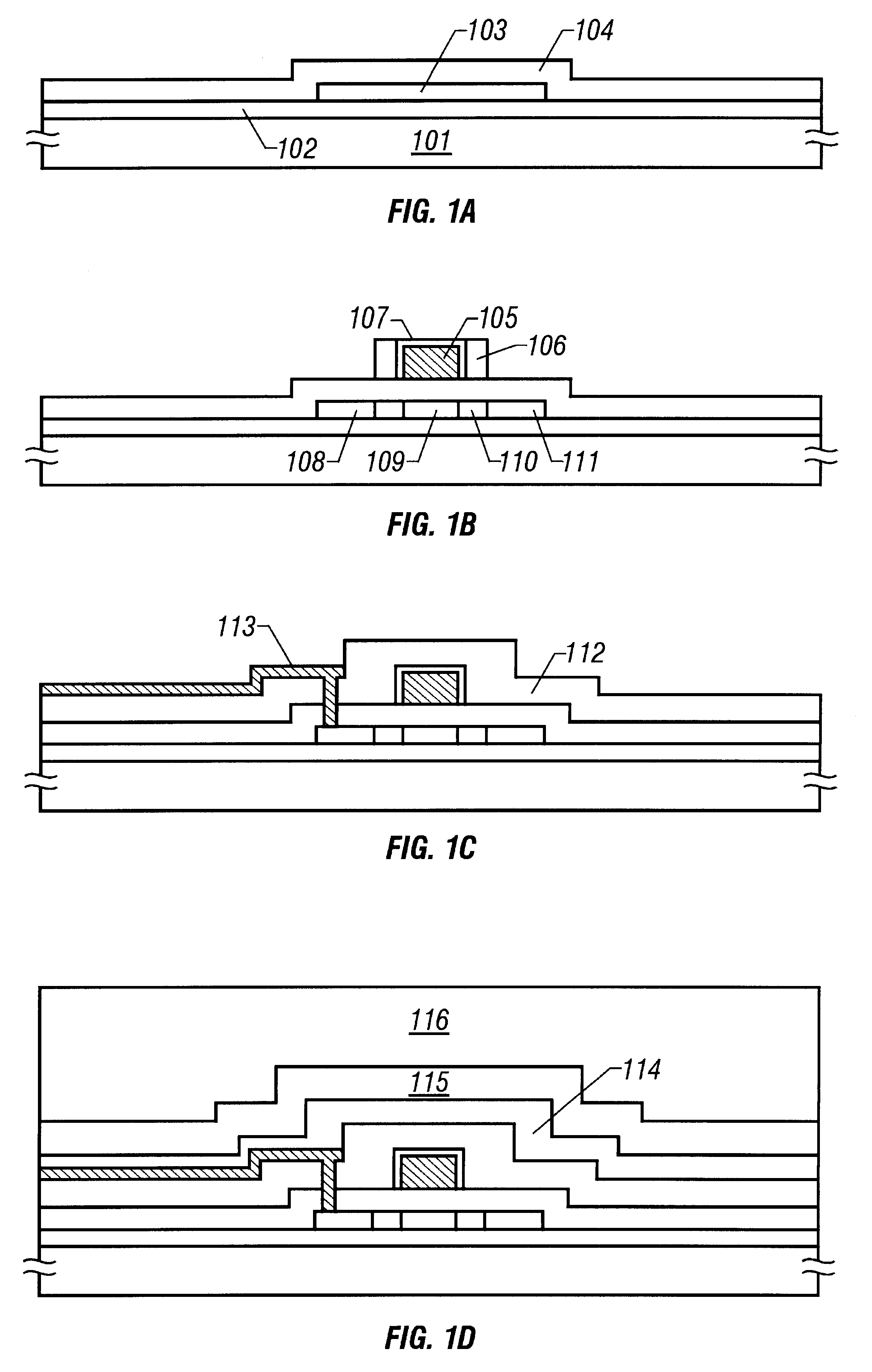
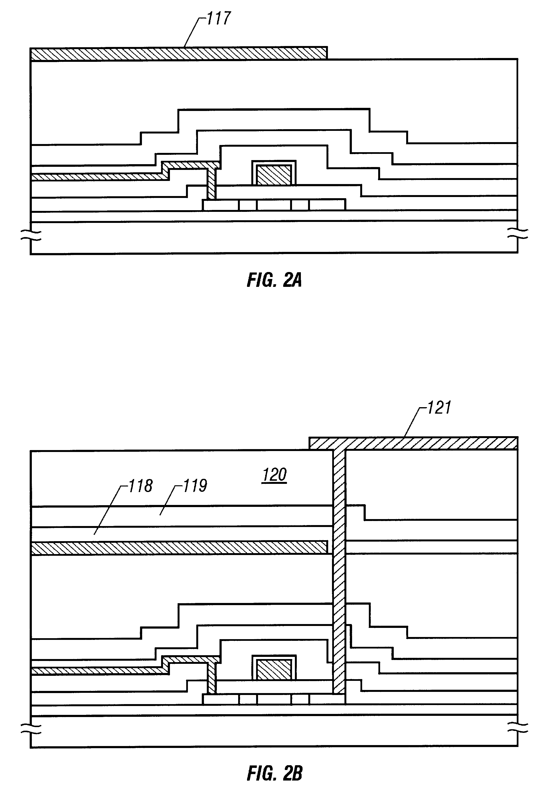
FIGS. 1 and 2 show steps of fabricating a pixel portion of an active matrix type liquid crystal display according to the present embodiment.
At first, a silicon oxide film 102 is formed in a thickness of 3000 .ANG. on a glass substrate 101 as an underlying layer by means of plasma CVD as shown in FIG. 1A. This underlying layer has a function of suppressing impurities from diffusing from the glass substrate to a semiconductor layer formed later. It also has a function of relaxing stress which acts between the glass substrate and the semiconductor layer formed later.
It is also useful to use a silicon oxynitride film for the underlying layer. Because the silicon oxynitride film is dense and has a high adhesiveness with the glass substrate, it is highly functional as the underlying layer.
The silicon oxynitride film may be formed by using mixed gas of silane, oxygen and N.sub.2 O by means of plasma CVD. It may be obtained by using mixed gas of TEOS gas and N.sub.2 O by m...
second embodiment
[Second Embodiment]
The present embodiment is characterized in that the structure illustrated in the first embodiment is improved further to increase the reliability.
As described above, a metallic material such as chrome is used for the light shielding film and black matrix However, when a long-term reliability is concerned, there may be problems of diffusion of impurities from the metallic material and of short-circuit caused between the metallic material and other electrodes and wires.
Then, in a structure illustrated in the present embodiment, an anodizable material is used for the light shielding film for shielding the thin film transistor and an anodic oxide film is formed on the surface thereof in addition to the structure illustrated in the first embodiment.
Aluminum or tantalum may be used as the anodizable material. When aluminum is used in particular, a suitable light shielding film may be formed because the anodic oxide film may be colored in black or in color close to that ...
third embodiment
[Third Embodiment]
The present embodiment relates to a structure in which aperture ratio of a pixel is increased further. Generally, it is desired to increase the aperture ratio of the pixel as much as possible. It is necessary to dispose the pixel electrode in a widest possible area in order to increase the aperture ratio of the pixel.
However, because capacity is produced between the pixel electrode and the thin film transistor and the wires when they are overlapped each other, it has been limited greatly in this aspect in general.
The present embodiment provides a structure for reducing the problem of producing the capacity.
FIG. 4 shows the structure of the present embodiment. In the structure shown in FIG. 4, source lines and gate lines disposed in a matrix are caused to function as a black matrix and an area of the pixel electrode 402 is increased as much as possible.
In the structure shown in FIG. 4, a light shielding film 401 for covering the main part of the thin film transistor...
PUM
 Abstract
Description
Claims
Application Information