
Power module

a power module and power electronics technology, applied in the direction of the association of semiconductor/solid-state devices, printed circuit non-printed electric components, electrical apparatus construction details, etc., can solve the problems of increasing the turn-off loss of the device, reducing the reliability of the device, and reducing the parasitic inductance and emi, so as to facilitate the power module structure, reduce the parasitic inductance and emi, the effect of reducing the parasitic in

Active Publication Date: 2022-05-31
DELTA ELECTRONICS (SHANGHAI) CO LTD
View PDF24 Cites 0 Cited by
  • Summary
  • Abstract
  • Description
  • Claims
  • Application Information

AI Technical Summary

Benefits of technology

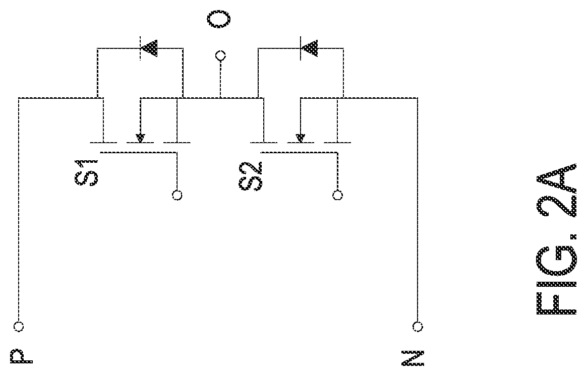
The present patent provides a carrier board and a power module using the same. The carrier board includes a main body with at least two terminals and at least one surface, at least two metal-wiring layers, and at least one metal block. The metal block is embedded in the main body and connected to one of the at least two terminals. The at least two parts of metal traces have a loop inductance of less than or equal to 1.4 nH when calculated at a frequency greater than 1 MHz. The power module includes the carrier board and a bridge arm formed by two switches connected in series. The arrangement of components optimizes the reduction of parasitic inductance and EMI, simplifies the assembly structure, reduces the cost, enhances the reliability, and improves the heat dissipation capacity. The metal conductive component is kept away from the trace of the carrier board to reduce the output capacitance and parasitic inductances. The optimized power module reduces the clamping inductance and improves the overall performance.

Problems solved by technology

Therefore, a higher voltage spike is caused by larger stray inductance when the current change rate keeps in constant.
The voltage spike will reduce the reliability of the device and increase turn-off-loss of the device.
Moreover, the voltage spikes not only affect the efficiency, but also cause the electromagnetic interference problems.
At the same time, due to the unavoidable presence of parasitic inductance in the power loop, the high switching frequency of the power device causes a rapid voltage change, which will cause the EMI in the circuit to exceed the standard.
Generally, a semiconductor device is the device with a lot of losses, and the tolerable temperature of the semiconductor device is limited within a certain range.
If the semiconductor device is operated over the limitation, the working ability of the semiconductor device might be lost, or the performance of the semiconductor device might be deteriorated sharply.
(3) Generally, the cost of heat dissipation accounts for a large proportion of the system cost.

Method used


Image

  • Power module
  • Power module
  • Power module

Examples


first embodiment

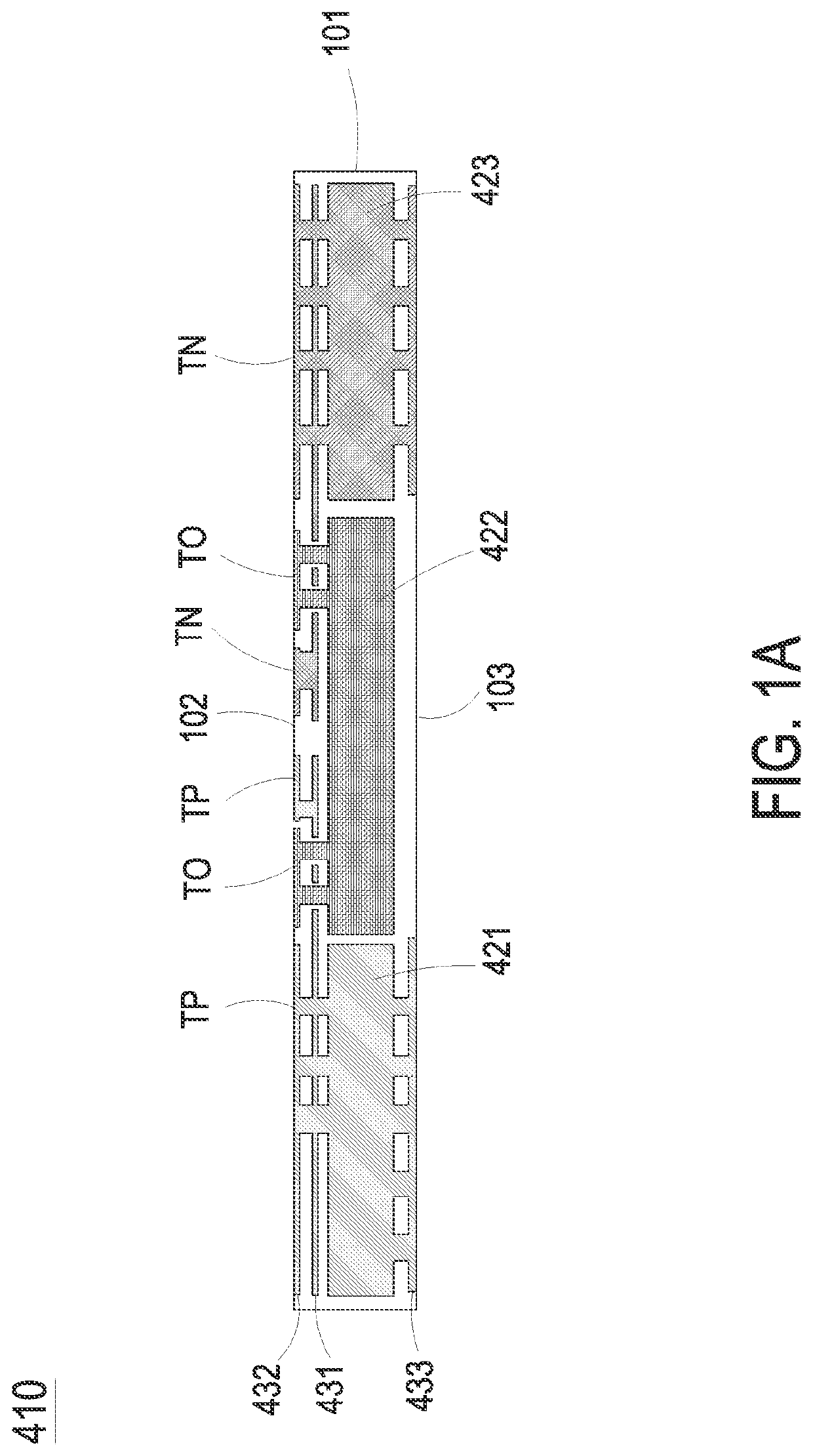
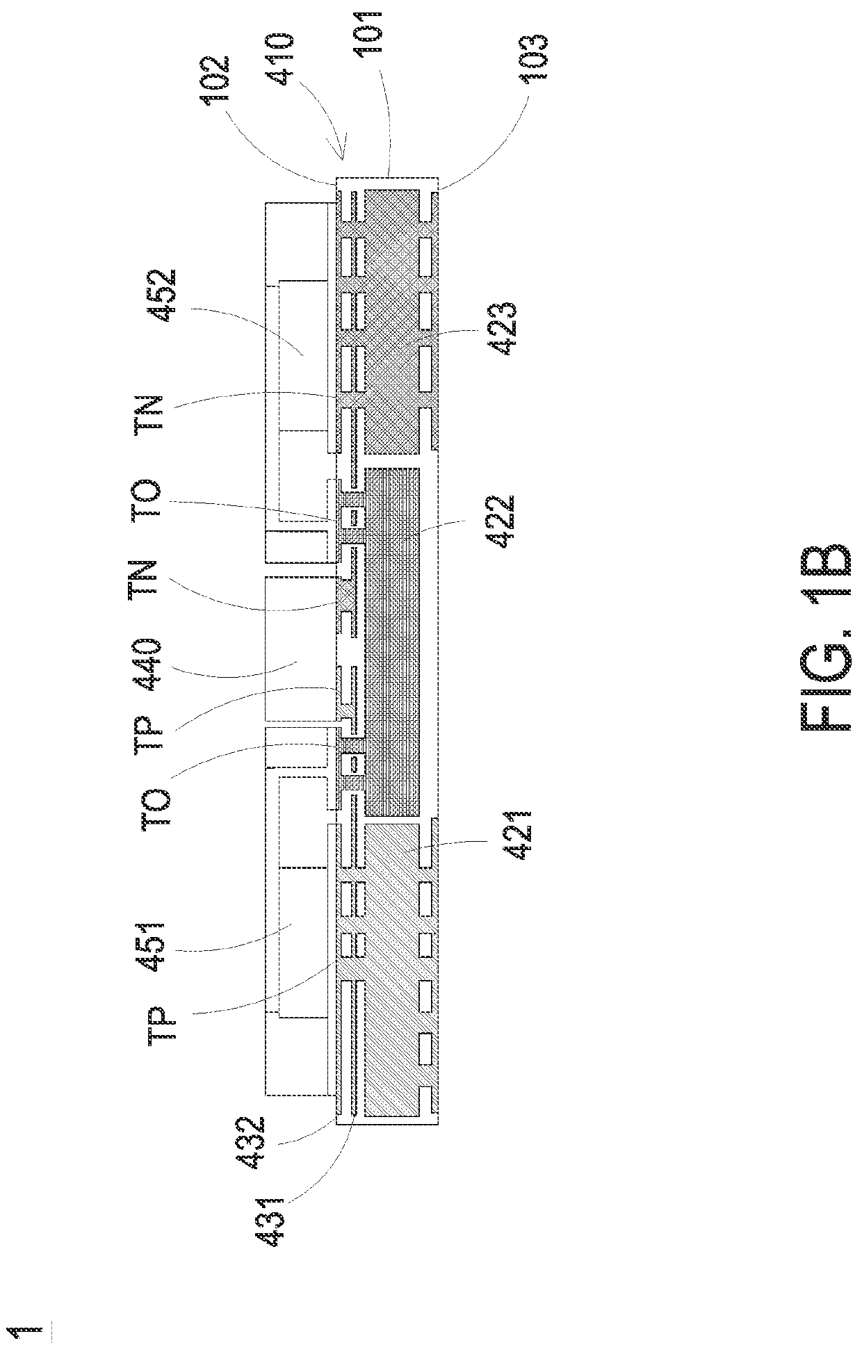
[0068]In order to achieve low parasitic inductance and good heat dissipation of a power devices or systems, the present disclosure provides a carrier board and a power module using the same. FIG. 1A is a schematic cross-sectional view illustrating a carrier board according to an embodiment of the present disclosure. FIG. 1B is a schematic cross-sectional view illustrating a power module according to the present disclosure. In the embodiment, the carrier board 410 of the power module 1 includes a main body 101, at least two metal-wiring layers (for example a first metal-wiring layer 431 and a second metal-wiring layer 432) and at least one metal block (for example a first metal block 421, a second metal block 422 and a third metal block 423). The main body 101 includes at least two terminals, an upper surface 102 and a lower surface 103. Preferably but not exclusively, the at least two terminals are selected from the at least two of a positive terminal TP, a negative terminal TN and ...

second embodiment

[0072]FIG. 4 is a top view illustrating a power module according to the present disclosure. FIG. 5 is a schematic cross-sectional view illustrating the power module of FIG. 4 and taken along the line A-A. FIG. 6 is a schematic cross-sectional view illustrating the power module of FIG. 4 and taken along the line C-C. FIG. 7 is a schematic cross-sectional view illustrating the power module of FIG. 4 and taken along the line B-B. FIG. 8 is a partial cross-sectional view illustrating the power module of FIG. 6 and taken along the line D-D. FIG. 9 is another partial cross-sectional view illustrating the power module of FIG. 6 and taken along the line D-D. In the embodiment, the structures, elements and functions of the power module 1a are similar to those of the power module 1 of FIG. 2, and are not redundantly described herein. In the embodiment, the power module 1a includes a carrier board 410, a first switch 451, a second switch 452 and a clamping component 440. The carrier board 410 ...

third embodiment

[0081]FIG. 11 is a schematic cross-sectional view illustrating a power module with a heat dissipation device according to the present disclosure. In the embodiment, the structures, elements and functions of the power module 1b are similar to those of the power module 1a of FIG. 5, and are not redundantly described herein. In the embodiment, the power module 1b further includes a first heat dissipation device 1002 and a first thermal-conductive and insulating material 1001. The first heat dissipation device 1002 and the first thermal-conductive and insulating material 1001 are disposed on the lower surface 103 of the carrier board 410. The first metal block 421, the second metal block 422, and the third metal block 423 are connected to the first heat dissipation device 1002 through the first thermal-conductive and insulating material 1001. As shown in FIG. 11, the first metal block 421, the second metal block 422, and the third metal block 423 are connected to the first heat dissipat...


PUM


Abstract

A power module is disclosed. The power module includes a carrier board, two switches, at least one metal block, a clamping component and a metal conductive component. The carrier board includes an upper surface and a lower surface. The two switches are disposed on the upper surface and connected in series to form a bridge arm electrically connected between a positive terminal and a negative terminal. The metal block is electrically connected to the two switches. The clamping component is disposed on the upper surface and electrically connected in parallel with the bridge arm through the carrier board. The metal conductive component is connected from a common node of the two switches to an output terminal. The metal conductive component is located at a side of the two switches facing away from the upper surface.

Description

CROSS-REFERENCE TO RELATED APPLICATION[0001]This application claims priorities to China Patent Application No. 202010075506.4, filed on Jan. 22, 2020, and China Patent Application No. 202110064810.3, filed on Jan. 18, 2021. The entire contents of the above-mentioned patent applications are incorporated herein by reference for all purposes.FIELD OF THE INVENTION[0002]The present disclosure relates to the field of power electronics, and more particularly to a power module.BACKGROUND OF THE INVENTION[0003]As an important part of power conversion, modern power electronic equipment is widely used in the power, electronics, motor and energy industries. Ensuring long-term stable operation of power electronic equipment and improving power conversion efficiency of power electronic equipment have been an important goal of those skilled in the art.[0004]As the core component of modern power electronic equipment, power semiconductor devices directly determine the reliability and power conversio...

Claims


Application Information

Patent Timeline
Patent Type & Authority Patents(United States)
IPC IPC(8): H05K7/00H05K1/02H05K1/09H05K1/11H05K1/18
CPCH05K1/0216H05K1/0203H05K1/09H05K1/111H05K1/181H05K2201/10166H01L25/072H01L23/5386H02M1/34H01L23/3677H01L23/5384H01L23/5383H01L23/36H05K1/0204H05K2201/10416H05K3/0061H01L2224/40245H01L24/40H01L2224/83801H01L2224/8384H01L2224/29101H01L2924/13091H01L2924/00014H01L24/48H01L2224/371H01L24/37H01L2224/73263H01L24/73H01L24/29H01L24/83H01L2924/181H01L2224/73265H01L2224/48247H01L2224/32245H01L2224/0603H01L2224/06181H01L2224/73221H01L2924/014H01L2224/45099H01L2924/00012H01L2924/00
Inventor HONG, SHOUYUXU, HAIBINWANG, TAOZHOU, WEICHENGJI, CHAOZHANG, WEIQIANG
Owner DELTA ELECTRONICS (SHANGHAI) CO LTD
Learn More