Fingerprint sensor and display device including the same

a fingerprint sensor and display device technology, applied in the field of fingerprint sensors and display devices, can solve the problems of increased manufacturing cost and increased thickness of display devices, and achieve the effects of reducing the thickness of the display device, maximizing the effective image area, and improving the efficiency and reliability of fingerprint sensing

Active Publication Date: 2022-05-03
SAMSUNG DISPLAY CO LTD
View PDF22 Cites 2 Cited by
  • Summary
  • Abstract
  • Description
  • Claims
  • Application Information

AI Technical Summary

Benefits of technology

[0006]Aspects of some example embodiments of the present disclosure may include a fingerprint sensor of a light sense method capable of reducing a manufacturing cost of a display device, and a display device including the fingerprint sensor.
[0030]According to some example embodiments, the fingerprint sensor and the display device including the fingerprint sensor may reduce a module thickness of the display device by integrally forming the light transmission area with the circuit element layer and the light emitting layer in the fingerprint sensor of a light sense type.
[0031]According to some example embodiments, the fingerprint sensor and the display device including the fingerprint sensor according to the disclosure may improve efficiency and reliability of fingerprint sensing by maximizing an effective image area.

Problems solved by technology

When such a fingerprint sensor is attached to a display panel, a thickness of the display device may increase and a manufacturing cost may increase.

Method used


Image

  • Fingerprint sensor and display device including the same
  • Fingerprint sensor and display device including the same
  • Fingerprint sensor and display device including the same

Examples


Embodiment Construction

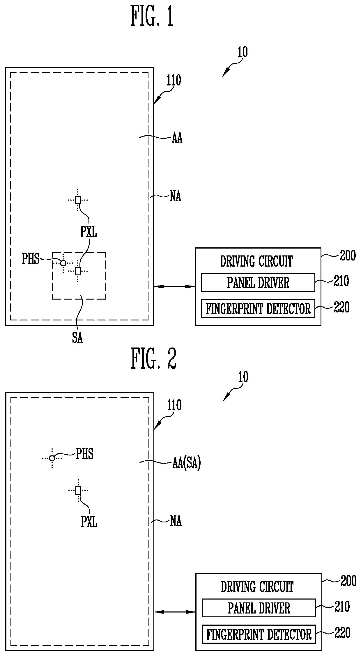
[0049]Hereinafter, aspects of some example embodiments of the disclosure will be described in more detail with reference to the accompanying drawings. The same or similar reference numerals are used for the same components in the drawings.

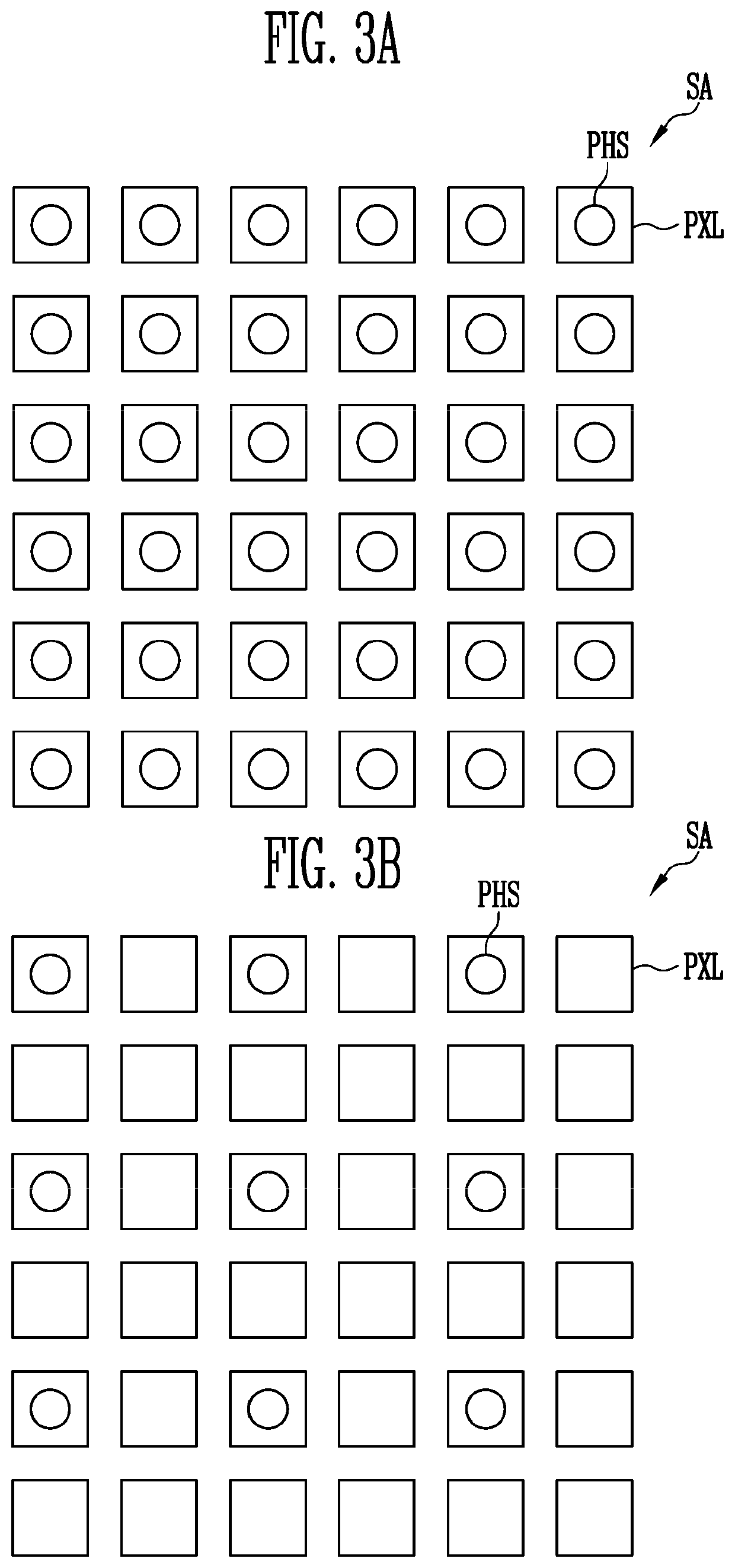
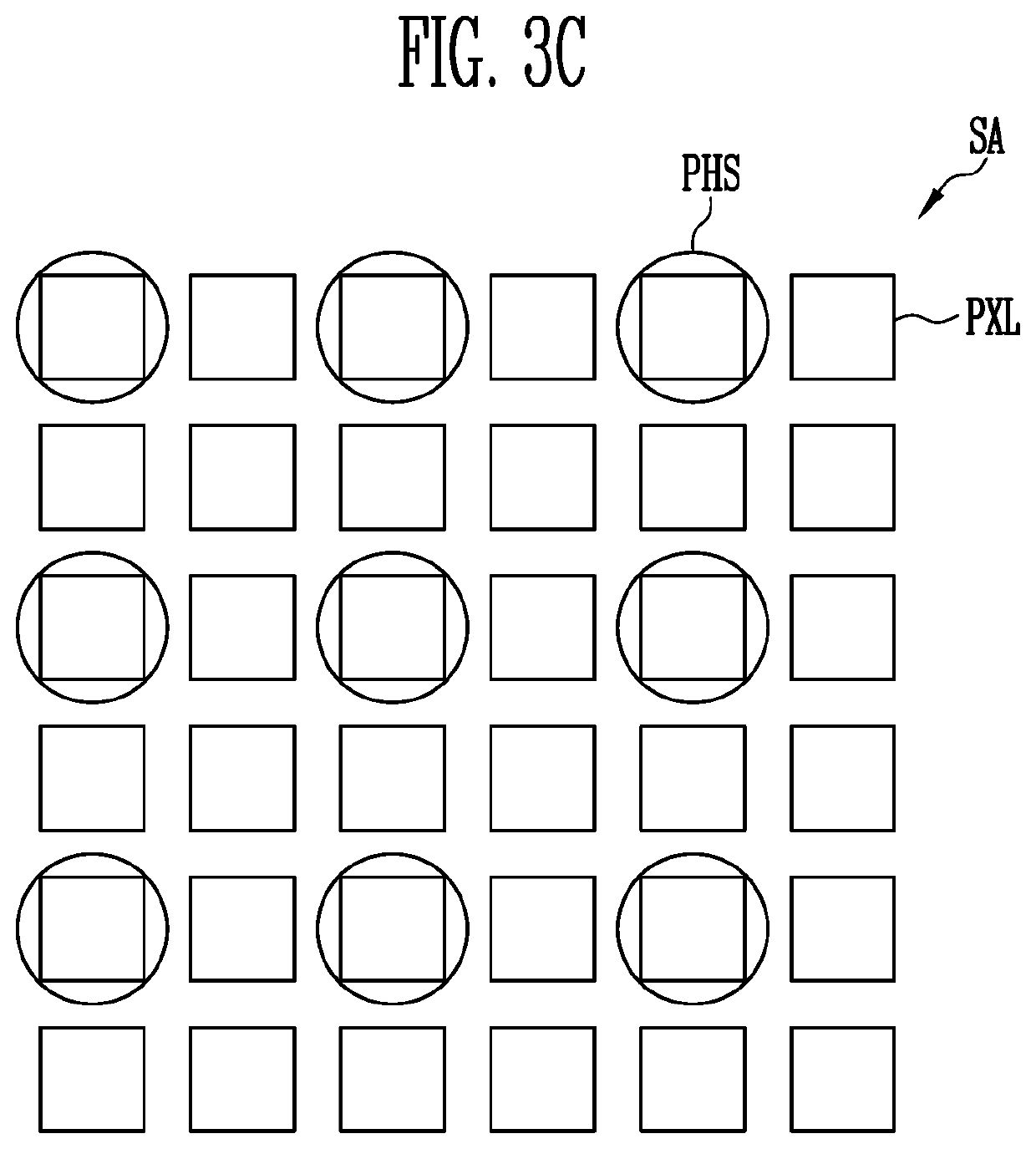
[0050]FIGS. 1 and 2 are diagrams schematically illustrating a display device according to some example embodiments of the disclosure. More specifically, FIGS. 1 and 2 are diagrams schematically illustrating a display panel included in a display device according to some example embodiments of the disclosure and a driving circuit for driving the display panel. For convenience, in FIGS. 1 and 2, the display panel and the driving circuit are separate from each other, but the disclosure is not limited thereto. For example, all or a part of the driving circuit may be integrally implemented on the display panel.

[0051]Referring to FIGS. 1 and 2, a display device 10 includes a display panel 110 and a driving circuit 200 for driving the display panel 110.

[00...


PUM

PropertyMeasurementUnit
distanceaaaaaaaaaa
distanceaaaaaaaaaa
distancesaaaaaaaaaa

Abstract

A fingerprint sensor includes: a substrate; a circuit element layer on a first surface of the substrate and including a plurality of conductive layers; a light emitting element layer on the circuit element layer and including light emitting elements and a light shielding layer; and a light sensor layer on a second surface of the substrate and including light sensors, wherein the light shielding layer includes contact holes exposing first electrodes of the light emitting elements, and first opening portions exposing a portion of the circuit element layer, and the circuit element layer includes second opening portions formed in the plurality of conductive layers and includes a light transmission hole of which at least a portion overlaps the first opening portions.

Description

CROSS-REFERENCE TO RELATED APPLICATION[0001]This application claims priority to and the benefit of Korean Patent Application No. 10-2019-0062644, filed on May 28, 2019, the content of which in its entirety is herein incorporated by reference.BACKGROUND1. Field[0002]Aspects of some example embodiments of the present disclosure relate to a fingerprint sensor and a display device including the fingerprint sensor.2. Description of the Related Art[0003]In recent years, as display devices such as smartphones or a tablet PCs have been widely used, biometric information authentication methods using a fingerprint of users may be used. In order to provide a fingerprint sensing function, a fingerprint sensor may be provided in a form embedded or attached to a display device.[0004]For example, the fingerprint sensor may be configured of a sensor of a light sense method. The fingerprint sensor of the light sense method may include a light source, a lens, and a light sensor array. When such a fin...

Claims


Application Information

Patent Timeline
Patent Type & Authority Patents(United States)
IPC IPC(8): G06F3/041H01L27/32G06K9/00H01L51/52
CPCH01L27/3227G06F3/0412G06K9/0004H01L27/3213H01L27/3246H01L51/5284G06V40/1324G06V40/1318G06V10/145G06V10/147H10K59/35H10K59/38H10K59/40H10K59/123H10K59/1213H10K59/1216H10K59/1315H10K59/122H10K59/353H10K59/65H10K59/121H10K50/865G06F3/041H10K59/60H10K59/12H10K50/80H10K59/351
Inventor RYU, JI HUNKWAG, JIN OH
Owner SAMSUNG DISPLAY CO LTD
Why Eureka
Try Eureka