Al technical title is built by PatSnap Al team. It summarizes the technical point description of the patent document.
a filter circuit and acoustic wave resonator technology, applied in the field of electronic devices, can solve the problems of driving rf complexity in smartphones, limitations of conventional rf technology, and the difficulty of using and transferring single crystal piezoelectric thin films
Active Publication Date: 2022-08-16
AKOUSTIS INC
View PDF74 Cites 8 Cited by
Summary
Abstract
Description
Claims
Application Information
AI Technical Summary
This helps you quickly interpret patents by identifying the three key elements:
Problems solved by technology
Method used
Benefits of technology
Benefits of technology
[0019]One or more benefits are achieved over pre-existing techniques using the invention. In particular, the present device can be manufactured in a relatively simple and cost effective manner while using conventional materials and / or methods according to one of ordinary skill in the art. The present device provides an ultra-small form factor RF resonator filter with high rejection, high power rating, and low insertion loss. Such filters or resonators can be implemented in an RF filter device, an RF filter system, or the like. Depending upon the embodiment, one or more of these benefits may be achieved.
Problems solved by technology
Coexistence of new and legacy standards and thirst for higher data rate requirements is driving RF complexity in smartphones.
Unfortunately, limitations exist with conventional RF technology that is problematic, and may lead to drawbacks in the future.
Even so, there are challenges to using and transferring single crystal piezoelectric thin films in the manufacture of BAWR and BAW filters.
Method used
Image
Click on the blue label to locate the original text in one second.
Reading with bidirectional positioning of images and text.
Examples
Embodiment Construction
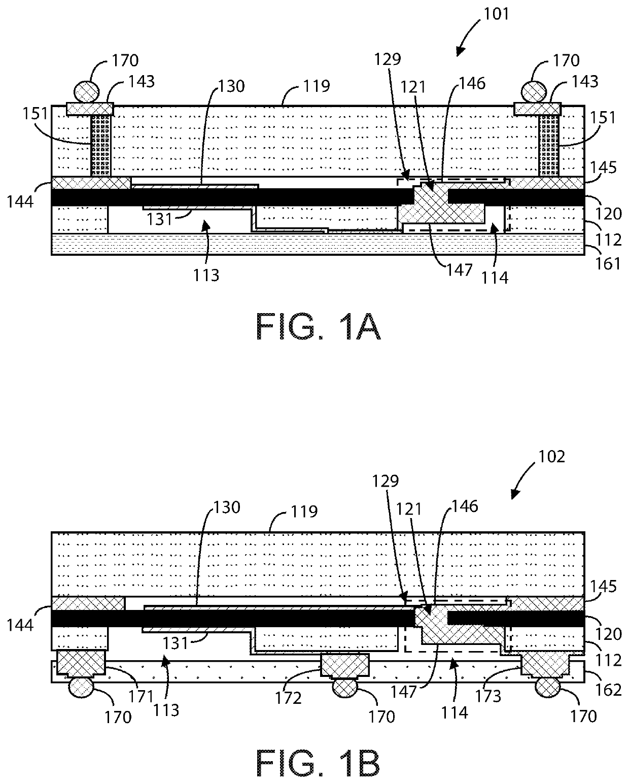
[0052]According to the present invention, techniques generally related to electronic devices are provided. More particularly, the present invention provides techniques related to a method of manufacture and structure for bulk acoustic wave resonator devices, single crystal resonator devices, single crystal filter and resonator devices, and the like. Merely by way of example, the invention has been applied to a single crystal resonator device for a communication device, mobile device, computing device, among others.
[0053]FIG. 1A is a simplified diagram illustrating an acoustic resonator device 101 having topside interconnections according to an example of the present invention. As shown, device 101 includes a thinned seed substrate 112 with an overlying single crystal piezoelectric layer 120, which has a micro-via 129. The micro-via 129 can include a topside micro-trench 121, a topside metal plug 146, a backside trench 114, and a backside metal plug 147. Although device 101 is depict...
PUM
Abstract
An RF circuit device using modified lattice, lattice, and ladder circuit topologies. The devices can include four resonator devices and four shunt resonator devices. In the ladder topology, the resonator devices are connected in series from an input port to an output port while shunt resonator devices are coupled to the nodes between the resonator devices. In the lattice topology, a top and a bottom serial configurations each includes a pair of resonator devices that are coupled to differential input and output ports. A pair of shunt resonators is cross-coupled between each pair of a top serial configuration resonator and a bottom serial configuration resonator. The modified lattice topology adds baluns or inductor devices between top and bottom nodes of the top and bottom serial configurations of the lattice configuration. These topologies may be applied using single crystal or polycrystalline bulk acoustic wave (BAW) resonators.
Description
CROSS-REFERENCES TO RELATED APPLICATIONS[0001]The present application claims priority to and is a continuation-in-part of U.S. application Ser. No. 16 / 290,703, filed Mar. 1, 2019, which is a continuation-in-part of U.S. application Ser. No. 16 / 175,650, filed Oct. 30, 2018, which is a continuation-in-part application of U.S. application Ser. No. 16 / 019,267, filed Jun. 26, 2018, which is a continuation-in-part application of U.S. application Ser. No. 15 / 784,919, filed Oct. 16, 2017 and now issued as U.S. Pat. No. 10,355,659 issued on Jul. 16, 2019, which is a continuation-in-part application of U.S. application Ser. No. 15 / 068,510, filed Mar. 11, 2016 and now issued as U.S. Pat. No. 10,217,930 issued on Feb. 26, 2019. The present application incorporates by reference, for all purposes, the following patent applications, all commonly owned: U.S. patent application Ser. No. 14 / 298,057, titled “RESONANCE CIRCUIT WITH A SINGLE CRYSTAL CAPACITOR DIELECTRIC MATERIAL”, filed Jun. 2, 2014; U....
Claims
Application Information
Patent Timeline
Application Date:The date an application was filed.
Publication Date:The date a patent or application was officially published.
First Publication Date:The earliest publication date of a patent with the same application number.
Issue Date:Publication date of the patent grant document.
PCT Entry Date:The Entry date of PCT National Phase.
Estimated Expiry Date:The statutory expiry date of a patent right according to the Patent Law, and it is the longest term of protection that the patent right can achieve without the termination of the patent right due to other reasons(Term extension factor has been taken into account ).
Invalid Date:Actual expiry date is based on effective date or publication date of legal transaction data of invalid patent.
