Touch display device and manufacturing method thereof
a technology of touch display and manufacturing method, applied in the field of displays, can solve the problem of exposed interior lines of the touch display module, and achieve the effect of reducing the number of touch display modules
- Summary
- Abstract
- Description
- Claims
- Application Information
AI Technical Summary
Benefits of technology
Problems solved by technology
Method used
Image


Examples
first embodiment
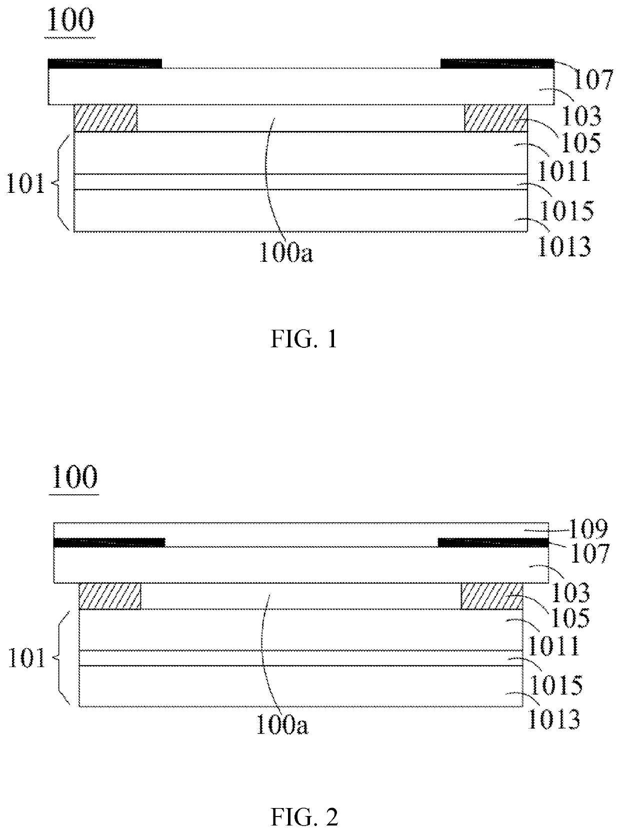
[0034]Please refer to FIG. 1 showing a schematic structural view of a touch display device of the present application. The touch display device 100 includes a touch display module 101, a protection cover 103, a sealant 105, a first shielding layer 107, and a chamber 100a.
[0035]The touch display module 101 includes a touch panel 1011, a display panel 1013, and an adhesive film layer 1015 disposed between the touch panel 1011 and the display panel 1013. The touch panel 1011 may include one of a capacitive touch component, a resistive touch component, an acoustic touch component, a mechanical touch component, and an optical touch component. In this embodiment, the touch panel 1011 includes the capacitive touch component. The display panel 1013 is a liquid crystal display panel or an organic light-emitting diode display panel. The adhesive film layer 1015 is adhered to the touch panel 1011 and the display panel 1013 in a comprehensive manner. The adhesive film layer 1015 is an optical ...
second embodiment
[0041]Please refer to FIG. 2 showing a schematic structural view of a touch display device of a first aspect of the present application. The touch display device 100 of FIG. 2 is substantially similar to the touch display device 100 of FIG. 1, except that the touch display device 100 further includes an anti-glare film (AG film) 109. The anti-glare film 190 is disposed on a side of the protection cover 103 away from the touch panel 1011. The anti-glare film 109 functions to prevent glare and reflection, and greatly enhances eye comfort of viewing the touch display device 100. The anti-glare film 109 is an anti-glare film. The anti-glare film 109 includes a polymer substrate and scattering particles coated on the polymer substrate. The polymer substrate is made of polyethylene terephthalate (PET).
[0042]Specifically, the first shielding layer 107 is disposed between the anti-glare film 109 and the protection cover 103. The first shielding layer 107 is formed on a surface of at least o...
third embodiment
[0045]Please refer to FIG. 4 showing a schematic structural view of a touch display device of a first aspect of the present application. The touch display device 100 of FIG. 4 is substantially similar to the touch display device 100 of FIG. 1, except that a chamber 100a is a vacuum chamber. The protection cover 103 is recessed into the chamber 100a from where the protection cover corresponds to the chamber, reducing a space of the chamber 100a, thereby improving users' touch feeling about the touch display device 100. The chamber 100a in cooperation with sealing property of the sealant 105 can further prevent dust, water vapor, and the like from entering the chamber 100a.
[0046]The touch display device 100 further includes a first anti-rainbow stripes layer 111 disposed between the touch panel 1011 and the protection cover 103. Specifically, the first anti-rainbow stripes layer 111 is disposed between the sealant 105 and the touch panel 1011. The first anti-rainbow stripes layer 111...
PUM
| Property | Measurement | Unit |
|---|---|---|
| shape | aaaaa | aaaaa |
| area | aaaaa | aaaaa |
| adhesion | aaaaa | aaaaa |
Abstract
Description
Claims
Application Information