Pedestal with a thermally controlled platen

a technology of thermal control and platen, which is applied in the direction of static indicating devices, instruments, coatings, etc., can solve the problems of cooling the wafer, the response time required to bring the wafer to the desired temperature is relatively long, and the gradients across the wafer surfa

Inactive Publication Date: 2001-06-28
APPLIED MATERIALS INC
View PDF0 Cites 268 Cited by
  • Summary
  • Abstract
  • Description
  • Claims
  • Application Information

AI Technical Summary

Benefits of technology

[0012] In another aspect of the invention, a processing system is provided. In one embodiment, a processing system includes a process chamber, a showerhead centrally disposed beneath a lid of the process chamber, a gas supply connected to the lid of the process chamber and a platen disposed within said process chamber. The process chamber includes walls having internal passages that are fluidly connected to a coolant reservoir. The platen includes a platen body having a plug centrally disposed in a workpiece support surface of the platen body. A lower surface of the plug defined a void between the plug and a bottom of the bore. The void creates a dichotomy of thermal paths through the platen body thus controlling the temperature of a wafer support surface.

Problems solved by technology

Changes in, and gradients across the wafer surface during wafer processing are detrimental to material deposition, etch rate, feature taper angles, step coverage and the like.
This method of cooling the wafer has two inherent problems.
First, the response times required to bring a wafer to a desired temperature is relatively long.
As such, rapid dynamic control of the water temperature to compensate for rapid wafer temperature fluctuations is not possible.
A second disadvantage of this method is the inability to control the temperature uniformity across the surface of the wafer.
This temperature gradient is one of the primary causes of feature variation in semiconductor wafer processing.
Such gradients between a plurality of devices cause substantial temperature variation across the wafer, i.e., hot and cold locations are formed.

Method used


Image

  • Pedestal with a thermally controlled platen
  • Pedestal with a thermally controlled platen
  • Pedestal with a thermally controlled platen

Examples


Embodiment Construction

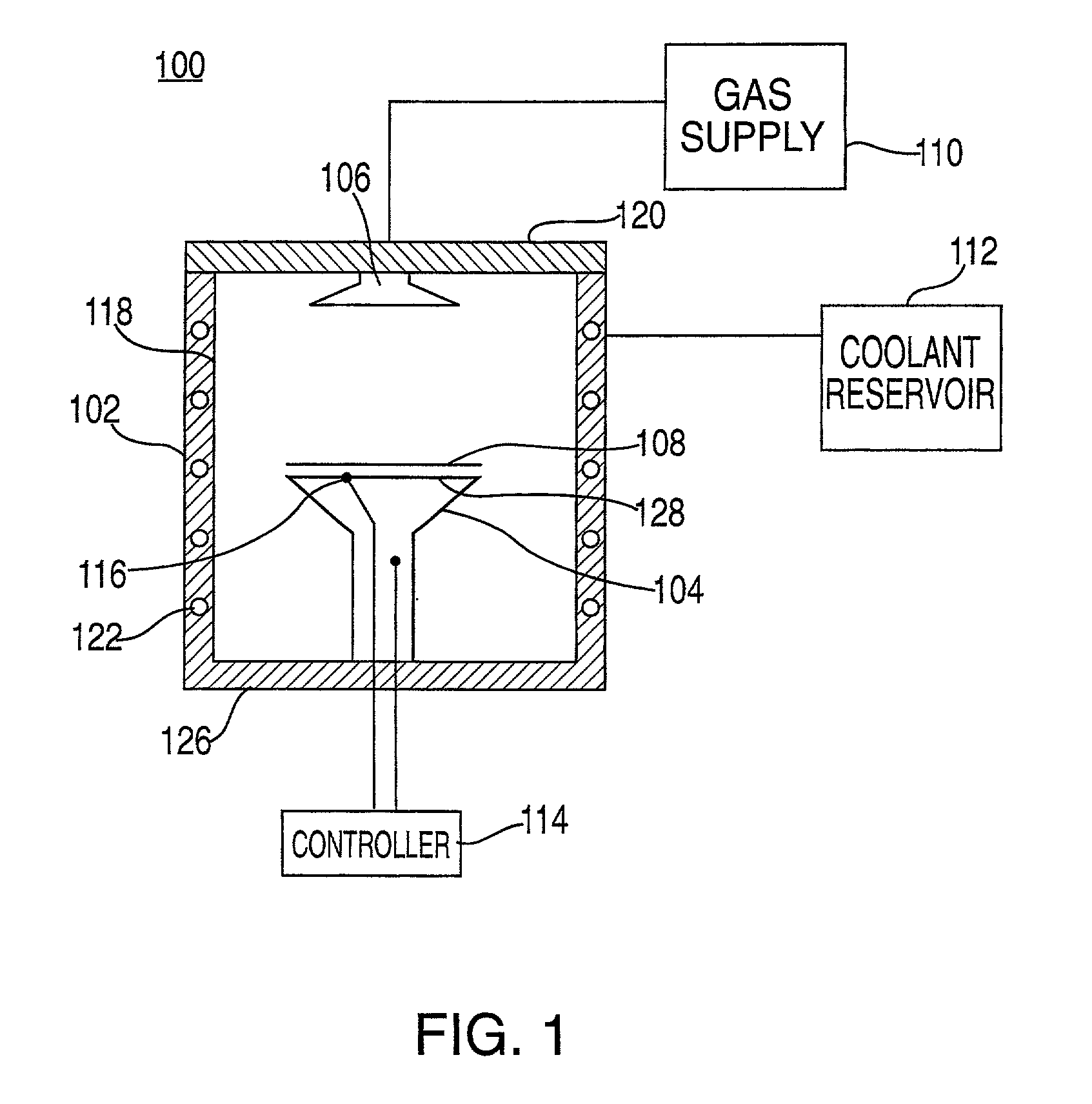
[0023] FIG. 1 depicts a cross-sectional schematic view of a semiconductor wafer processing system 100. The depicted system is, for example, a chemical vapor deposition (CVD) system. However, such a system is merely illustrative of the invention's usefulness in any wafer processing system requiring that the wafer be maintained at a uniform temperature. The system 100 contains a process chamber 102, a pedestal assembly 104, a showerhead 106, a gas supply 110, a coolant reservoir 112, and a controller 114. The process chamber 102 has a base 126, wall 118 and a lid 120. A coolant (e.g., facility's water) circulates between the reservoir 112 and the chamber 102, flowing through passages 122 in the wall 118. The pedestal assembly 104 is disposed within the process chamber 102 and centered beneath the showerhead 106. The showerhead 106 provides a disbursive entry conduit for reactive and other gases to enter the chamber 102 from the gas supply 110. The pedestal assembly 104 contains a sens...


PUM

PropertyMeasurementUnit
diameteraaaaaaaaaa
pressureaaaaaaaaaa
angleaaaaaaaaaa

Abstract

A workpiece support having dichotomy of thermal paths therethrough is provided for controlling the temperature of a workpiece support thereon. In one embodiment, a workpiece support includes a platen body having a plug centrally disposed in a workpiece support surface of the platen body. A lower surface of the plug defines a void between the plug and a bottom of the bore. The void creates a dichotomy of thermal paths through the platen body thus controlling the temperature of a wafer support surface. Alternatively, the plug and platen body may be fabricated from materials having different rates of thermal conductivity to created the dichotomy of thermal paths in addition to or in absence of the void.

Description

[0001] This application is a continuation of co-pending U.S. patent application Ser. No. 09 / 349,412, filed Jul. 7, 1999, which is hereby incorporated by reference in its entirety.BACKGROUND OF THE DISCLOSURE[0002] 1. Field of Invention[0003] The present invention relates generally to a semiconductor wafer processing apparatus. More specifically, the invention relates to an apparatus for providing a controllable, uniform temperature distribution across the diameter of a semiconductor wafer.[0004] 2. Background of the Invention[0005] In semiconductor wafer processing, the surface temperature of the wafer is a critical process parameter. Changes in, and gradients across the wafer surface during wafer processing are detrimental to material deposition, etch rate, feature taper angles, step coverage and the like. It is essential to have control over local temperature uniformity during wafer processing to enhance processing and minimize undesirable characteristics.[0006] A number of device...

Claims


Application Information

Patent Timeline
Patent Type & Authority Applications(United States)
IPC IPC(8): C23C16/458C23C16/46H01L21/00
CPCC23C16/4586C23C16/46H01L21/67109Y10S156/915
Inventor CHO, THOMAS K.ISHIKAWA, TETSUYA
Owner APPLIED MATERIALS INC
Why Eureka
Try Eureka