SOI-structure MIS field-effect transistor and method of manufacturing the same

a soi-structure and field-effect transistor technology, applied in the field of metal insulator semiconductor (mis) field-effect transistors, can solve the problems of inability to achieve the effect of reducing power consumption, errors in the operation of the circuitry comprising the soi structure, and used in practi

Inactive Publication Date: 2001-08-23
SEIKO EPSON CORP
View PDF0 Cites 88 Cited by
  • Summary
  • Abstract
  • Description
  • Claims
  • Application Information

AI Technical Summary

Problems solved by technology

This causes various problems in the MOS field-effect transistor, such as the kink phenomenon and the parasitic bipolar effect.
However, a DTMOS has another problem in that it can only be used in practice under low gate voltage conditions of a gate voltage on the order of 1 V or less.
This current will make it impossible to achieve the lower power consumption that is the objective of a SOI structure.
Such a current would cause errors in the operation of the circuitry comprising the SOI structure.
In addition, since a small forward-direction current flows between the body region and the source region, even when the DTMOS is used at a gate voltage of less than 0.7 V, this impedes any reduction in the power consumption.

Method used


Image

  • SOI-structure MIS field-effect transistor and method of manufacturing the same
  • SOI-structure MIS field-effect transistor and method of manufacturing the same
  • SOI-structure MIS field-effect transistor and method of manufacturing the same

Examples


Embodiment Construction

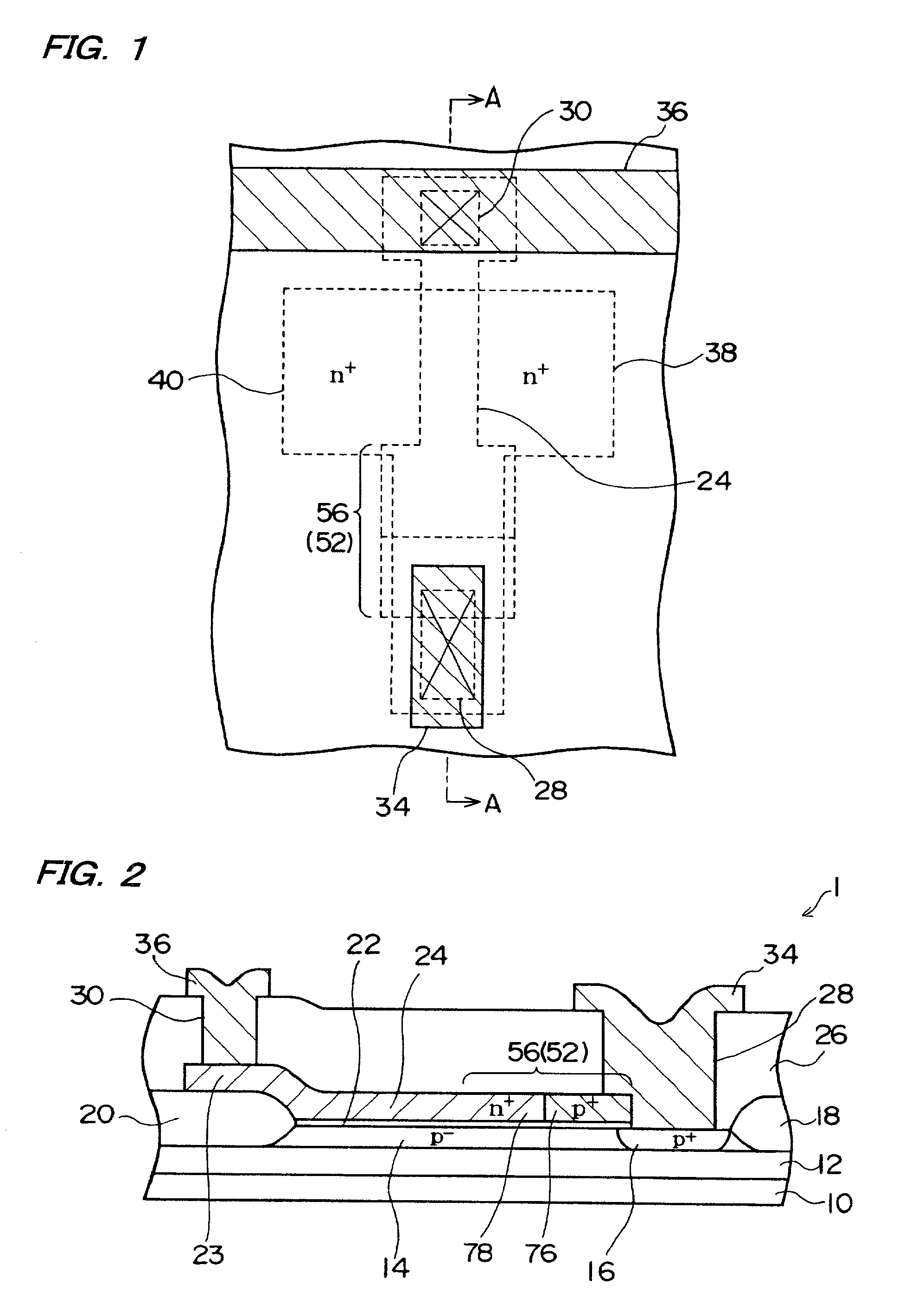
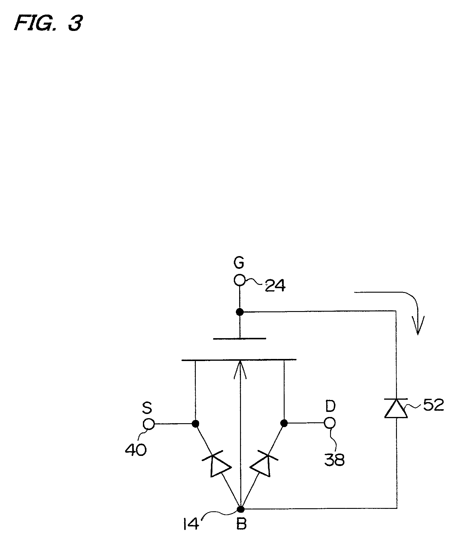
[0163] The effects produced by the provision of a resistance portion R will now be described with reference to experimental examples, together with the characteristics of a DTMOS. The resistance portion R described below was made of polysilicon. On the other hand, the PN junction portion of the present invention was made to function as the resistance portion R. Since either configuration can function as a resistor, it can be assumed that the present invention can achieve effects that are similar to those of these experimental examples. A schematic view of a conventional SOI-structure MOS field-effect transistor is shown in FIG. 32. This configuration has been described already in the Background of the Invention and is hereinafter called a floating-body type of field-effect transistor. A schematic view of another conventional SOI-structure MOS field-effect transistor is shown in FIG. 33. This configuration has been described already in the Background of the Invention and is hereinaft...


PUM


Abstract

A SOI-structure MOS field-effect transistor. In this transistor, agate electrode and a p- region that is a body region are placed into electrical contact by a PN junction portion. An n+-type portion of the PN junction portion is in electrical contact with the gate electrode and a p+-type portion of the PN junction portion is in electrical contact with a p- region. When a positive voltage is applied to the gate electrode, the above configuration ensures that a reverse voltage is applied to the PN junction portion, so that only a small current on the order of the reverse leakage current of the PN junction flows along the path from the gate electrode, to the PN junction portion and the body region, and into the source region.

Description

[0001] 1. Field of the Invention[0002] The present invention relates to a metal insulator semiconductor (MIS) field-effect transistor of a silicon-on-insulator (SOI) structure, and a method of manufacture thereof.[0003] 2. Description of Related Art[0004] A SOI-structure MOS field-effect transistor can be driven at a lower power consumption and a higher speed than an ordinary MOS field-effect transistor.[0005] A schematic view of an example of a conventional SOI-structure MOS field-effect transistor is shown in FIG. 32. A buried oxide film 1100 formed of a silicon oxide layer is formed on a silicon substrate 1000. A source region 1200 and a drain region 1300 are provided in mutually separate locations on the buried oxide film 1100. A body region 1400 is formed on the buried oxide film 1100, between the source region 1200 and the drain region 1300. A gate electrode 1500 is formed on the body region 1400 with a gate insulation film therebetween.[0006] The body region 1400 of the MOS f...

Claims


Application Information

Patent Timeline
Patent Type & Authority Applications(United States)
IPC IPC(8): H01L29/423H01L29/49H01L29/786
CPCH01L29/42384H01L29/4908H01L29/78609
Inventor EBINA, AKIHIKO
Owner SEIKO EPSON CORP
Why Eureka
Try Eureka