Methods and circuits for stacking bus architecture
a stacking bus and circuit technology, applied in the direction of transmission, unauthorized memory use protection, instruments, etc., can solve the problems of signal loss, physical limitations that must be accounted for, and it is almost impossible to find a office in the united states
- Summary
- Abstract
- Description
- Claims
- Application Information
AI Technical Summary
Problems solved by technology
Method used
Image
Examples
Embodiment Construction
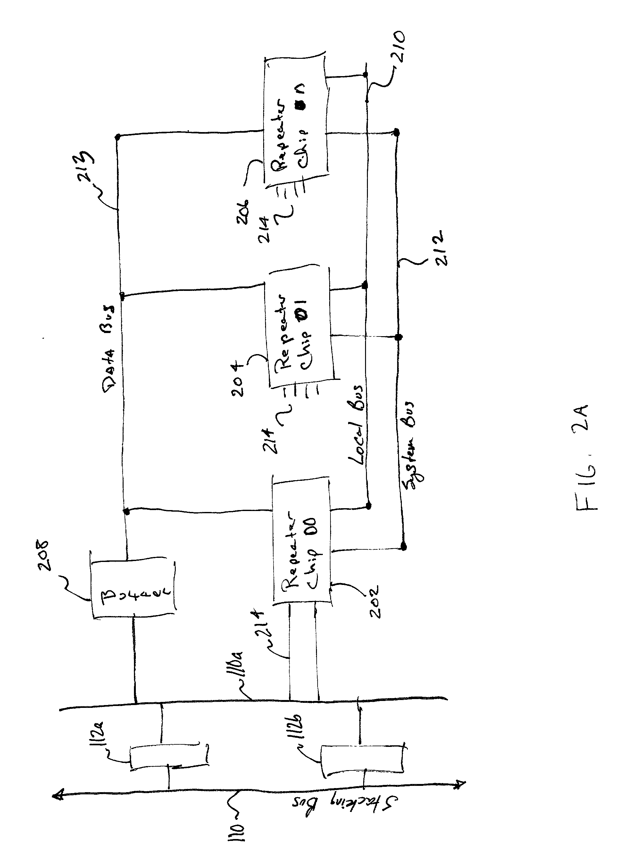
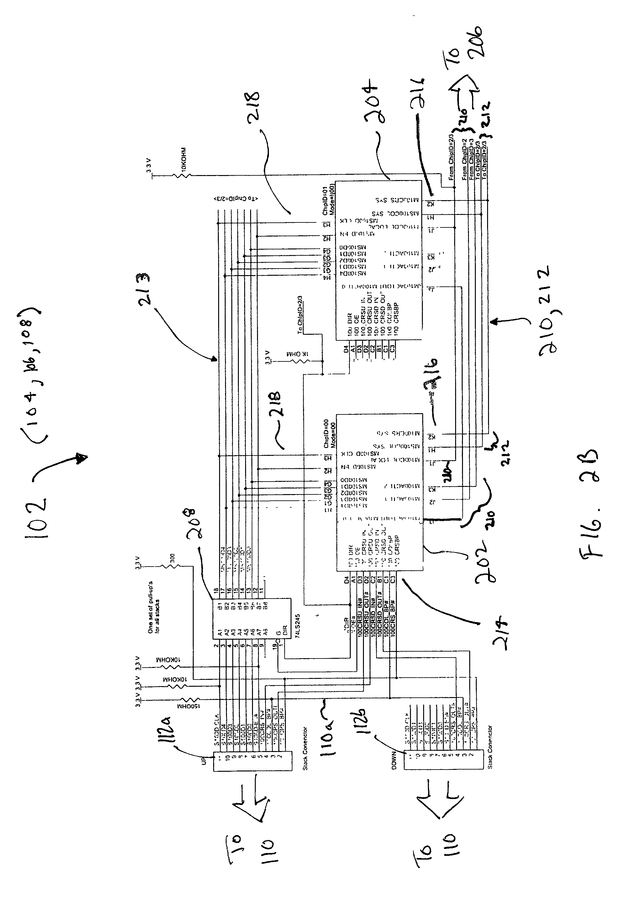
, two chips within one repeater receive a packet from the network at the same time. When a chip receives a packet from the network via its physical ports, for example chip 204, the chip sends a local carrier signal (CRS_LOCAL) to the master chip 202 via local bus 210. In the configuration according to FIG. 2B, the master chip 202 has a separate pin 216 (J3, J2, K3) to listen for status signals from each slave chip. Each slave chip drives its J3 pin to send a CRS_LOCAL signal to the master chip 202. Assuming that a second slave chip receives a signal at the same time, for example chip 206, chip 206 would likewise send a CRS_LOCAL signal to master chip 202 via local bus 210. Master chip 202 is configured to determine that a collision exists when it receives two or more signals from pins J3, J2, or K3, or if it receives one signal from pins J3, J2, or K3 and a data packet is received at a port of the master chip 202 at the same time. Once a collision is determined across a single repea...
PUM
 Abstract
Description
Claims
Application Information


