Non-contact thickness-measuring device
a technology of thickness measurement and non-contact, which is applied in the direction of lapping machines, instruments, manufacturing tools, etc., can solve the problem of lowering the quality of semiconductor wafers when their thickness is measured
- Summary
- Abstract
- Description
- Claims
- Application Information
AI Technical Summary
Problems solved by technology
Method used
Image
Examples
Embodiment Construction
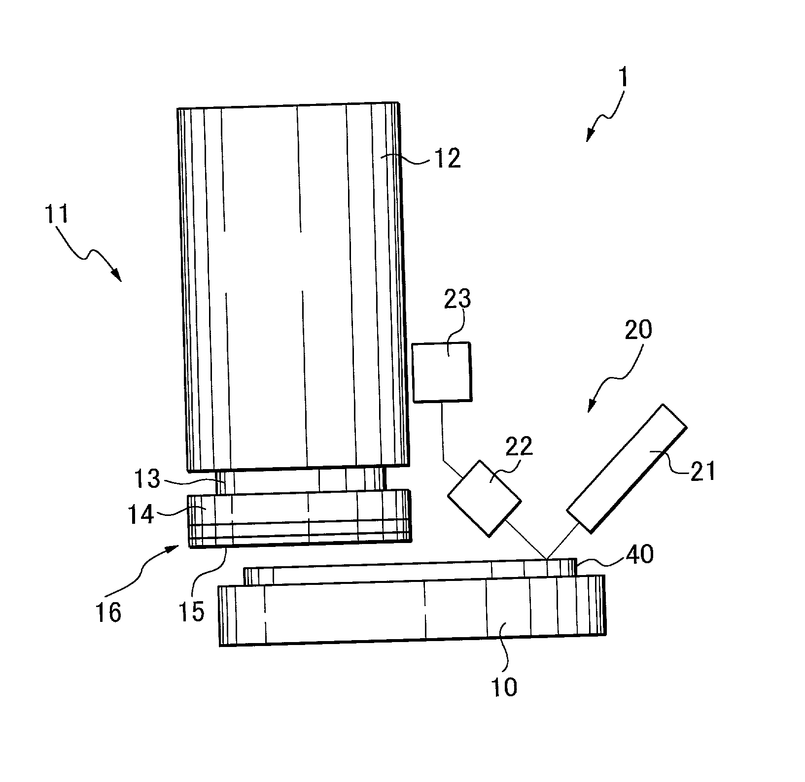
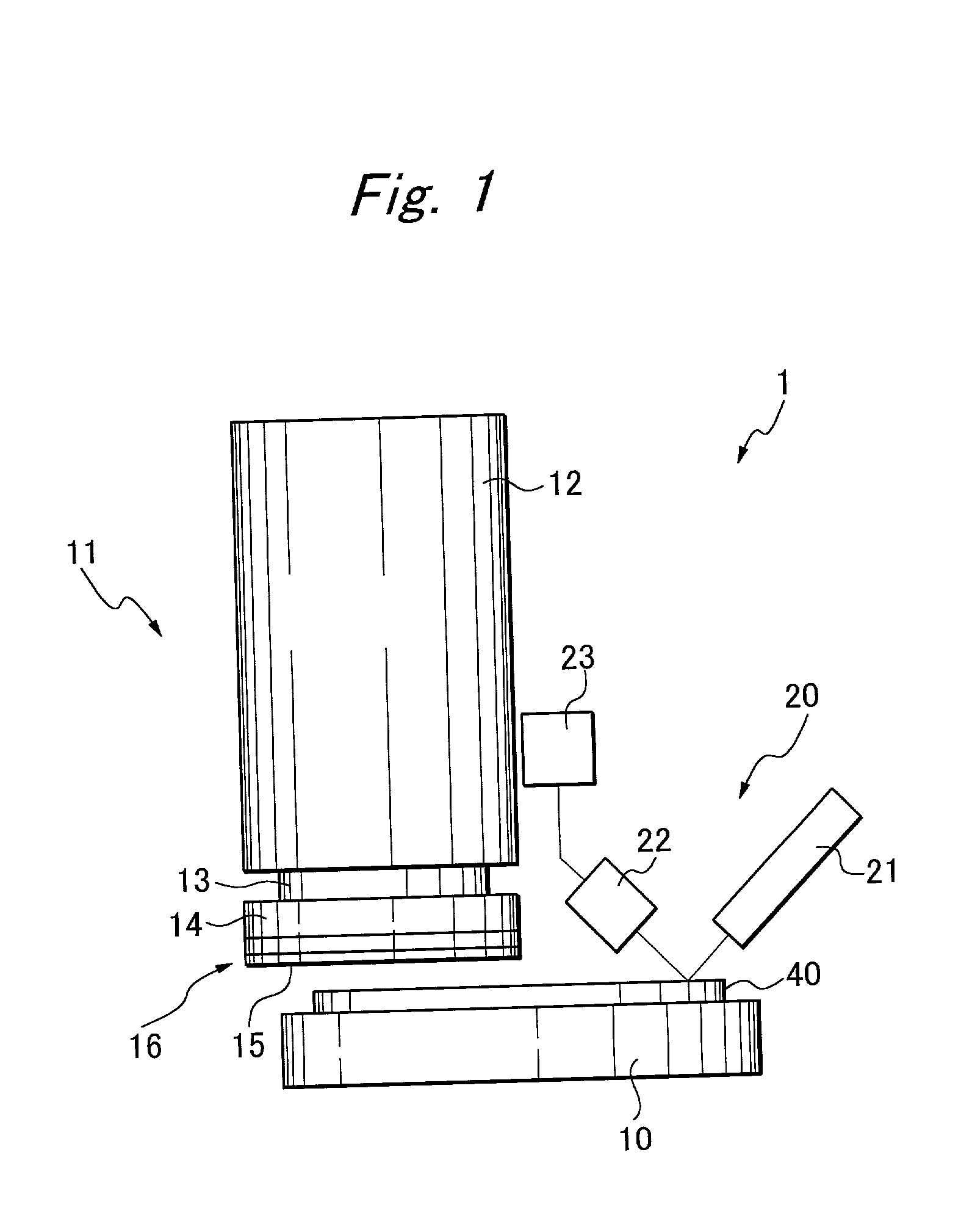
[0021] Referring to FIGS. 1 and 2, in which same parts as appear in FIG. 4 are indicated by same reference numerals, a workpiece 40 is fixedly held by the chuck table 10, and the grind stone 14 is fixed to the tip of the spindle 13 via the mount 14, and the spindle 13 is rotatably supported by the spindle housing 12.
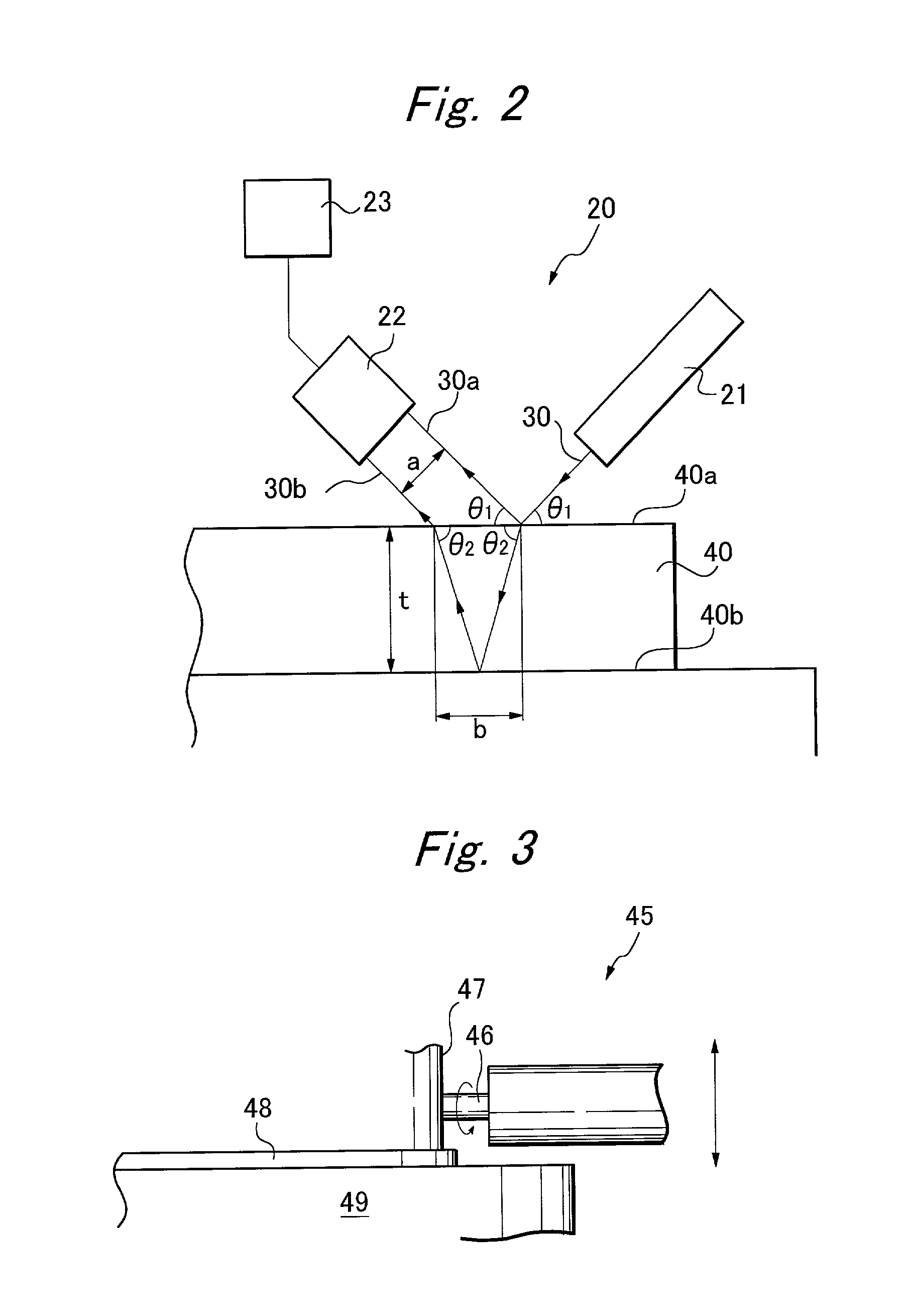
[0022] A laser light projecting means 21 is so placed in the vicinity of the workpiece 40 that the ray of laser light may be thrown to the workpiece 40 obliquely, and a imaging means 22 is so placed that the ray of laser light may fall on the imaging means 22 after being reflected on the top surface of the workpiece 40. The imaging means 22 is connected to an arithmetic means 23 for determining the thickness of the workpiece from the distance "a" between the first point at which the first ray of laser light 30a falls on the imaging means 22 and the second point at which the second ray of laser light 30b falls on the imaging means 22.
[0023] In FIG. 2, the ray of laser lig...
PUM
 Abstract
Description
Claims
Application Information


