Apparatus for plasma processing

a technology for processing apparatuses and plasma, applied in the direction of electric discharge tubes, chemical vapor deposition coatings, coatings, etc., can solve the problems of excessive increase in manufacturing costs, abnormal discharge of electricity in the apparatus, and complicated apparatus structure, so as to prevent the deformation of the slot antenna and uniform plasma

Inactive Publication Date: 2002-10-17
TOKYO ELECTRON LTD +3
View PDF2 Cites 15 Cited by
  • Summary
  • Abstract
  • Description
  • Claims
  • Application Information

AI Technical Summary

Benefits of technology

0032] The sixteenth feature of the present invention resides in that the slot antenna is held by struts each made of a dielectric material. With this structure, it is possible to produce a uniform plasma.
0033] The seve

Problems solved by technology

However, since cables inside the coaxial waveguide are easy to be heated in the above processing apparatus 71, such an overheating operation may cause an abnormal discharging of electricity in the apparatus.
However, this countermeasure would cause the structure of the apparatus to be complicated with an excessive increase in manufacturing cost.
Additi

Method used


Image

  • Apparatus for plasma processing
  • Apparatus for plasma processing
  • Apparatus for plasma processing

Examples


Embodiment Construction

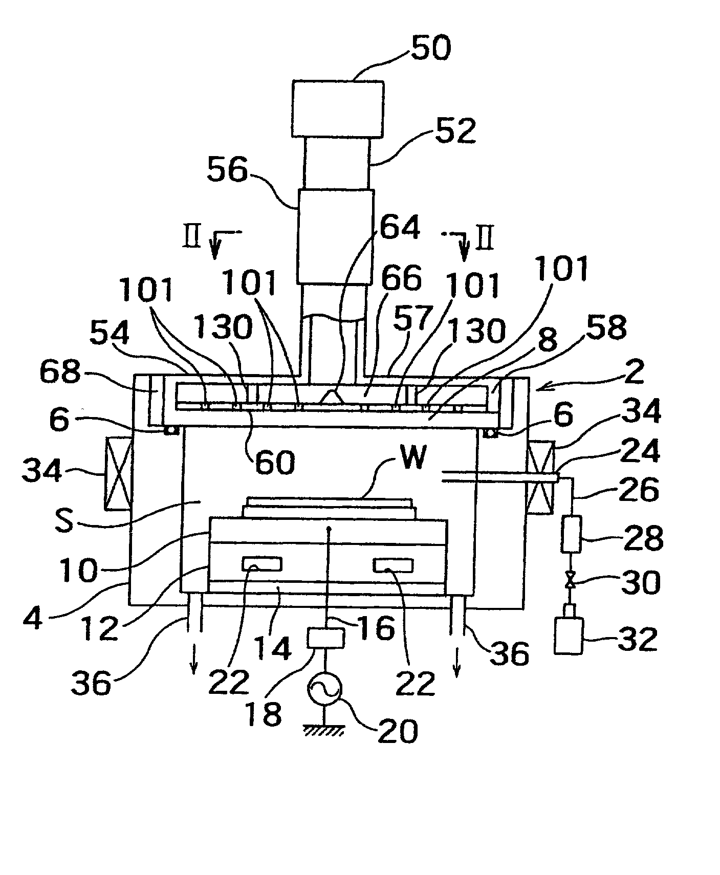
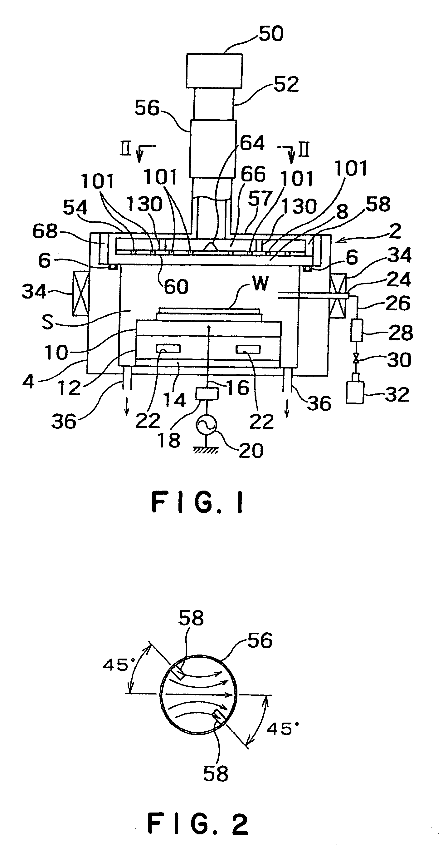
[0073] With reference to attached drawings, a plasma processing apparatus in accordance with one embodiment of the present invention will be described below, in detail. FIG. 1 is a sectional view of an example of the plasma processing apparatus of the present invention. FIG. 2 is a view showing a section of a circularly polarized wave converter, taken along a line II-II of FIG. 1.

[0074] Although the plasma processing apparatus is embodied by a plasma etching apparatus in this embodiment, it is a matter of course that the present invention is not limited to this example only. The plasma etching apparatus 2 includes a processing container 4 having its sidewall and bottom made of a conductive material, such as aluminum, and shaped to be a cylinder with a bottom as a whole. The ceiling part of the processing container 4 is opened. A silica plate 8 having a thickness to endure a vacuum pressure is disposed on the opened ceiling part through a sealing member 6, such as O-ring, in an airti...


PUM

PropertyMeasurementUnit
Dielectric polarization enthalpyaaaaaaaaaa
Diameteraaaaaaaaaa
Frequencyaaaaaaaaaa

Abstract

A plasma processing apparatus is provided. The plasma processing apparatus can generate a uniform plasma in a processing container to perform a uniform processing on even a large-diameter wafer. The apparatus includes a processing container 4 shaped to be a cylinder with a bottom and accommodating amounting table 10 for mounting a wafer W thereon, a silica plate 8 for covering an upper opening of the processing container 4 in an airtight manner, a microwave supplier 50 for supplying a microwave in TE11 mode and a cylindrical waveguide 52 having one end connected to the microwave supplier 50 to extend toward the silica plate 8 and also having an interior waveguide space. The apparatus further includes a radial waveguide box 54 connected to the other end of the cylindrical waveguide 52. The radial waveguide box 54 is shaped to extend from the other end of the cylindrical waveguide 52 radially outward in the form of a flange and successively extend toward a lid body downward as a sidewall to define an interior waveguide space. The apparatus further includes a disc-shaped slot antenna 60 arranged along the silica plate 8 to cover an opening at the lower end of the radial waveguide box 54 and have a plurality of slots 101, a circularly polarized wave converter 56 disposed in the cylindrical waveguide 52 between the microwave supplier 50 and the radial waveguide box 54 to rotate the TE11-mode microwave provided from the supplier 50 about an axis of the cylindrical waveguide 52 and send the rotating microwave to the radial waveguide box 54.

Description

TECHNICAL FIELD OF THE INVENTION[0001] The present invention relates to a plasma processing apparatus utilizing a microwave.BACKGROUND OF THE INVENTION[0002] Conventionally, there is known a plasma processing apparatus which includes a flat antenna, as shown in FIG. 18.[0003] This plasma processing apparatus 71 comprises a processing container 73 generally shaped to be cylindrical with a bottom and a silica plate 75 formed on the ceiling part of the processing container 73 in an airtight manner thereby to define a closed processing space S in the processing container 73. Accommodated in the processing container 73 is a mounting table 77 on which a semiconductor wafer W is mounted. This mounting table 77 is connected to a bias high-frequency power source 79 through power lines. Further, a gas nozzle 81 is arranged in the sidewall of the processing container 73, for introducing a process gas into the container. The processing container 73 is also provided, on a bottom thereof, with ex...

Claims


Application Information

Patent Timeline
IPC IPC(8): H01J37/32
CPCH01J37/3222H01J37/32229H01J37/32256H01J37/32247H01J37/3299
Inventor ISHII, NOBUOYASAKA, YASUYOSHISHINOHARA, KIBATSU
Owner TOKYO ELECTRON LTD
Why Eureka
Try Eureka