Capacitive circuit array for fingerprint sensing

a circuit array and fingerprint sensing technology, applied in the field of two-dimensional mapping of finger print patterns, can solve the problems of complex and expensive, large size, and inability to maintain thin membranes,

Inactive Publication Date: 2002-10-24
SENTRONICS CORP
View PDF0 Cites 23 Cited by
  • Summary
  • Abstract
  • Description
  • Claims
  • Application Information

AI Technical Summary

Problems solved by technology

In the area of the fingerprint sensor, the primary prior art systems utilizes an optical scanning method which is relatively bulky and expensive due to the optics, lasers and the CCD array utilized.
The first two categories are complex and expensive to make, and thus most of recent development activities are in the area of capacitive sensors.
However, such thin membranes are not durable, and hence, are not yet marketable.
The circuitry utilized in Tartagni et al, and Aukland et al, involve several transistors, an amplifier or charge accumulation and transfers in every pixel, making the sensor array essentially a large silicon chip and expensive to manufacture.
When a uniform finger surface is in contact, the fields cancel and pick up pad reads a null signal, but if there is a surface ridge, the fields are imbalanced and the pick up pad picks up a signal.

Method used


Image

  • Capacitive circuit array for fingerprint sensing
  • Capacitive circuit array for fingerprint sensing
  • Capacitive circuit array for fingerprint sensing

Examples


Embodiment Construction

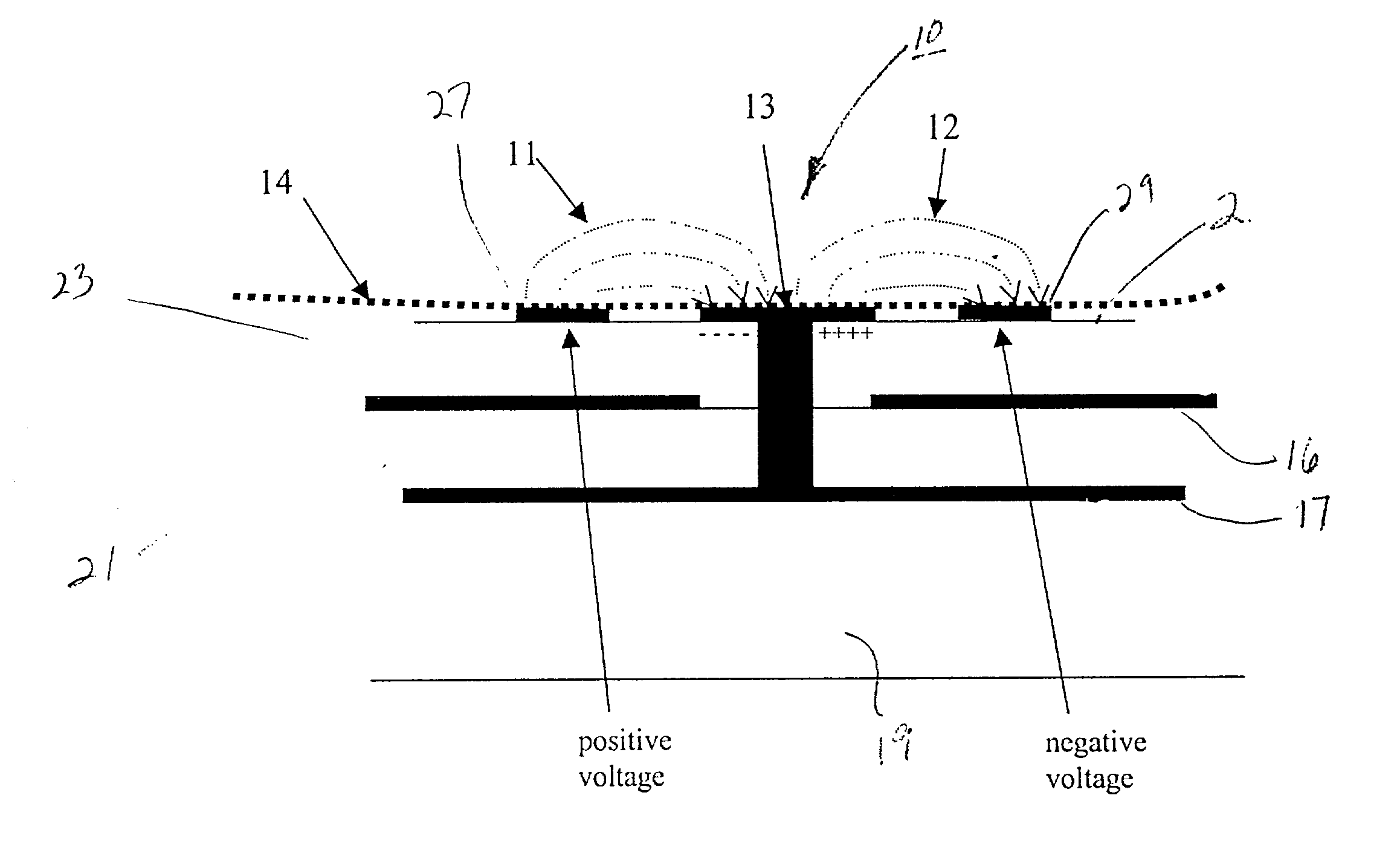
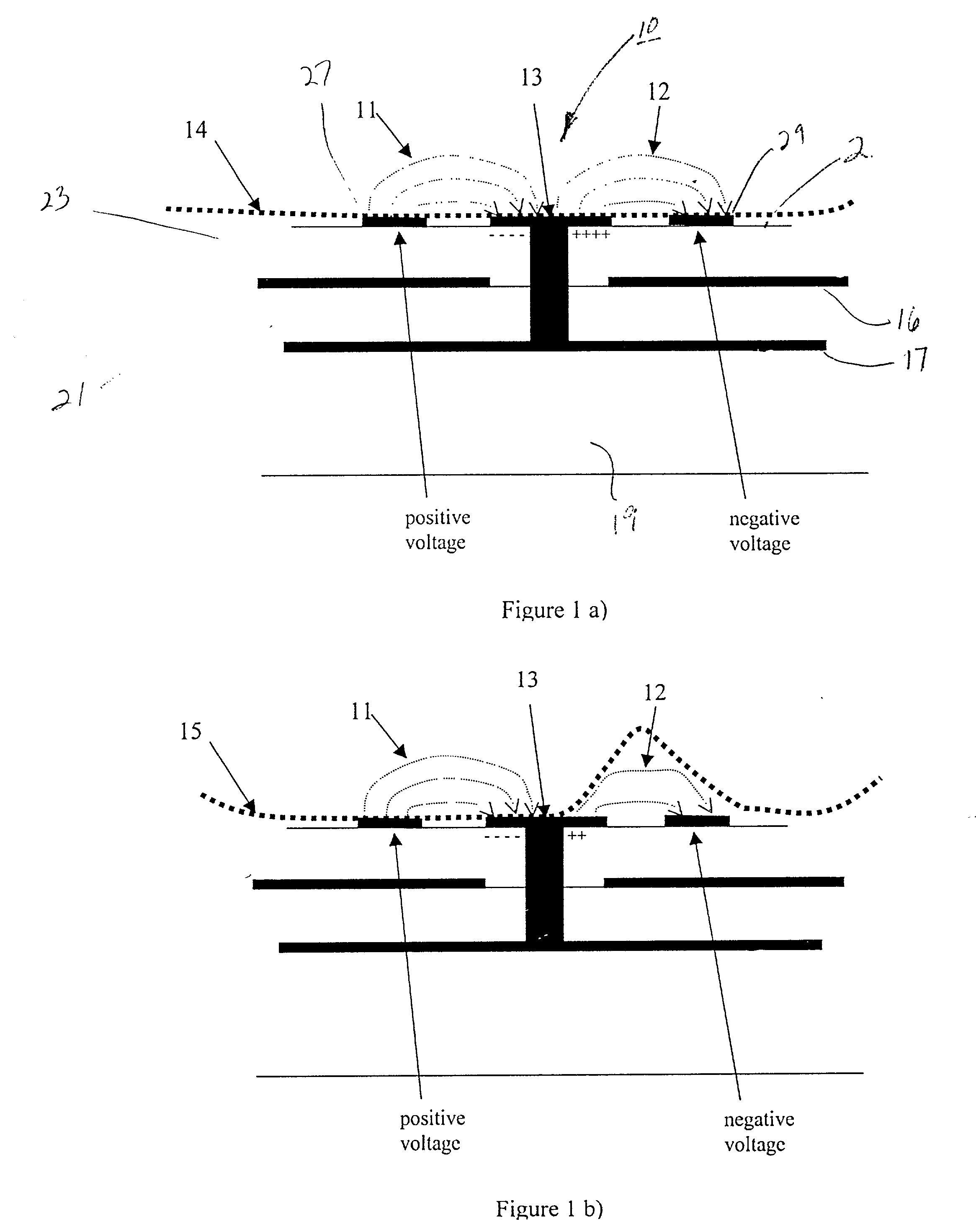
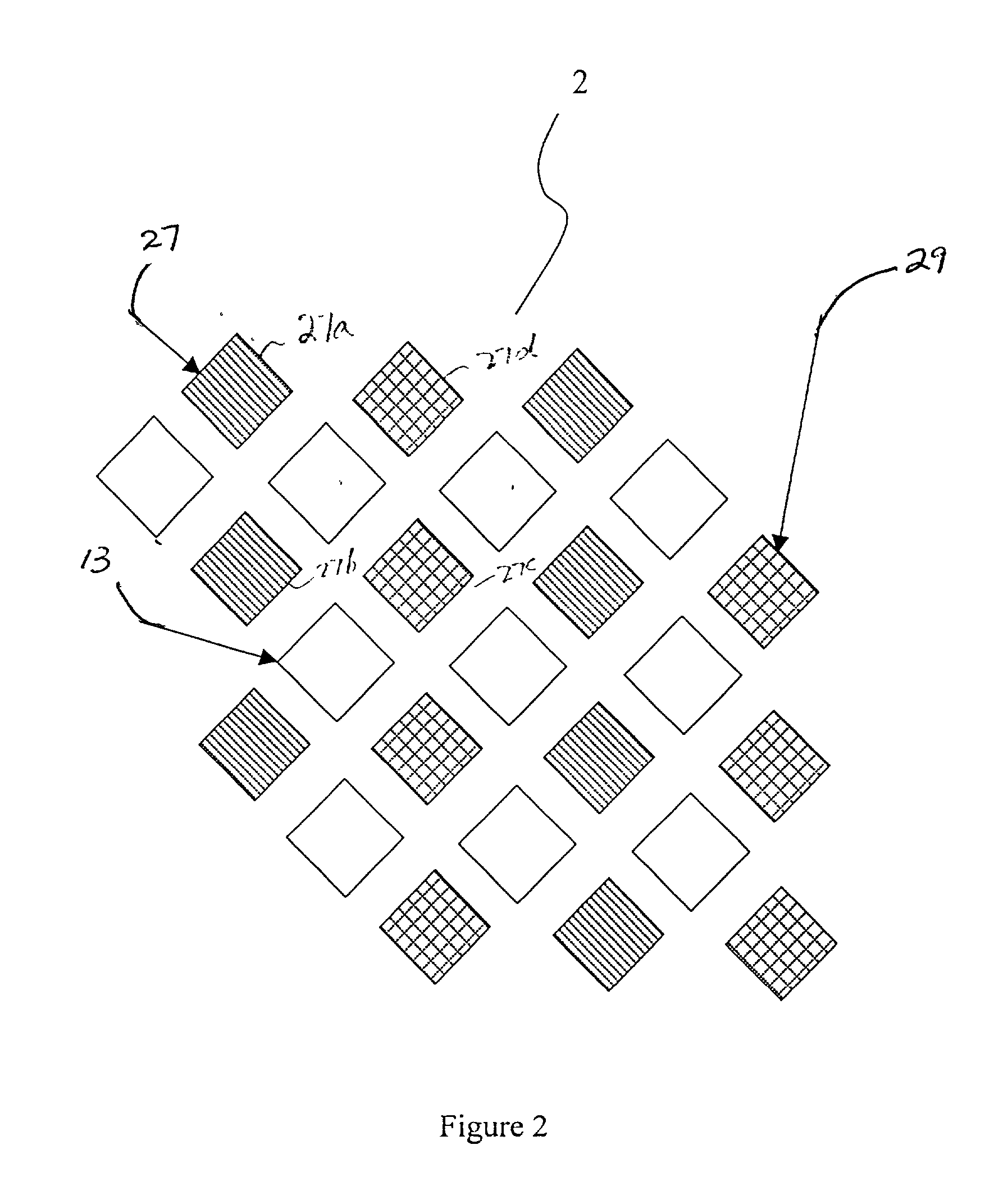
[0016] FIGS. 1(a) and 1(b) show a simplified version of the basic sensor device 10 of the present invention. Diametrically opposing fields 11 and 12 are generated within a pixel 10 (one point of the array) of the sensor array across pick up pad 13 by external voltage drivers, and when the contact surface 14 is uniform, the charges induced on the pick up pad 13 are zero or close to zero as shown in FIG. 1a (note that although only one pixel is illustrated, the actual device comprises a two-dimensional array of pixels). However, if the surface in contact 15 is non-symmetric, as shown in FIG. 1(b), then the fields become distorted and the induced charges on the pick up pad 13 do not cancel, and the pick up pad 13 registers a signal which is interpreted as the presence of a finger surface ridge. Pixel 10 further comprises shield 16, signal lines 17, substrate 19, insulation layers 21 and 23 and electrode pads 27 and 29 (a positive voltage is applied to pad 27; a negative voltage is appl...


PUM


Abstract

A low cost capacitive fingerprint sensor which can be fabricated on various substrates, such as large glass or plastic substrates. The sensor is made by depositing and patterning alternate layers of conductive and insulation materials. A pixel of the sensor is comprised of a pick up pad and a plurality of voltage electrodes symmetrically placed around the pick up pad. The symmetry is such that only when a finger surface ridge is present, the pick up pad registers a signal.

Description

[0001] 1. Field of the Invention[0002] The present invention relates to two dimensional mapping of finger print patterns for identification purposes utilizing a capacitive circuit array.[0003] 2. Description of the Prior Art[0004] Fingerprint sensing and the associated identification systems which include data bases and a match algorithm processor have been available in the prior art. In the area of the fingerprint sensor, the primary prior art systems utilizes an optical scanning method which is relatively bulky and expensive due to the optics, lasers and the CCD array utilized. Due to this reason, there have been attempts to develop electronic means of sensing fingerprint patterns. All electronic fingerprint sensors can be categorized as follows; tactile pressure sensors, thermal sensors and capacitive sensors. The first two categories are complex and expensive to make, and thus most of recent development activities are in the area of capacitive sensors.[0005] One group of capacit...

Claims


Application Information

Patent Timeline
Patent Type & Authority Applications(United States)
IPC IPC(8): G06K9/00
CPCG06K9/0002G06V40/1306
Inventor HAYES, ROBERT S.UM, GREGORY S.
Owner SENTRONICS CORP
Why Eureka
Try Eureka