Structure of a chip package

Inactive Publication Date: 2003-01-23
OPCOM
View PDF0 Cites 23 Cited by
  • Summary
  • Abstract
  • Description
  • Claims
  • Application Information

AI Technical Summary

Problems solved by technology

When other hard circuit boards are connected with the lens assembly, the body, after packaging, is extended but the components cannot be bent or minimized in volume.
However, after the assembly 1 is externally mounted with other PCB, the body of the lens assembly 1 becomes rather huge.
Further, the conventional package structure includes

Method used


Image

  • Structure of a chip package
  • Structure of a chip package
  • Structure of a chip package

Examples


Embodiment Construction

[0018] For the purpose of promoting an understanding of the principles of the invention, reference will now be made to the embodiment illustrated in the drawings. Specific language will be used to describe same. It will, nevertheless, be understood that no limitation of the scope of the invention is thereby intended, alterations and further modifications in the illustrated device, and further applications of the principles of the invention as illustrated herein being contemplated as would normally occur to one skilled in the art to which the invention relates.

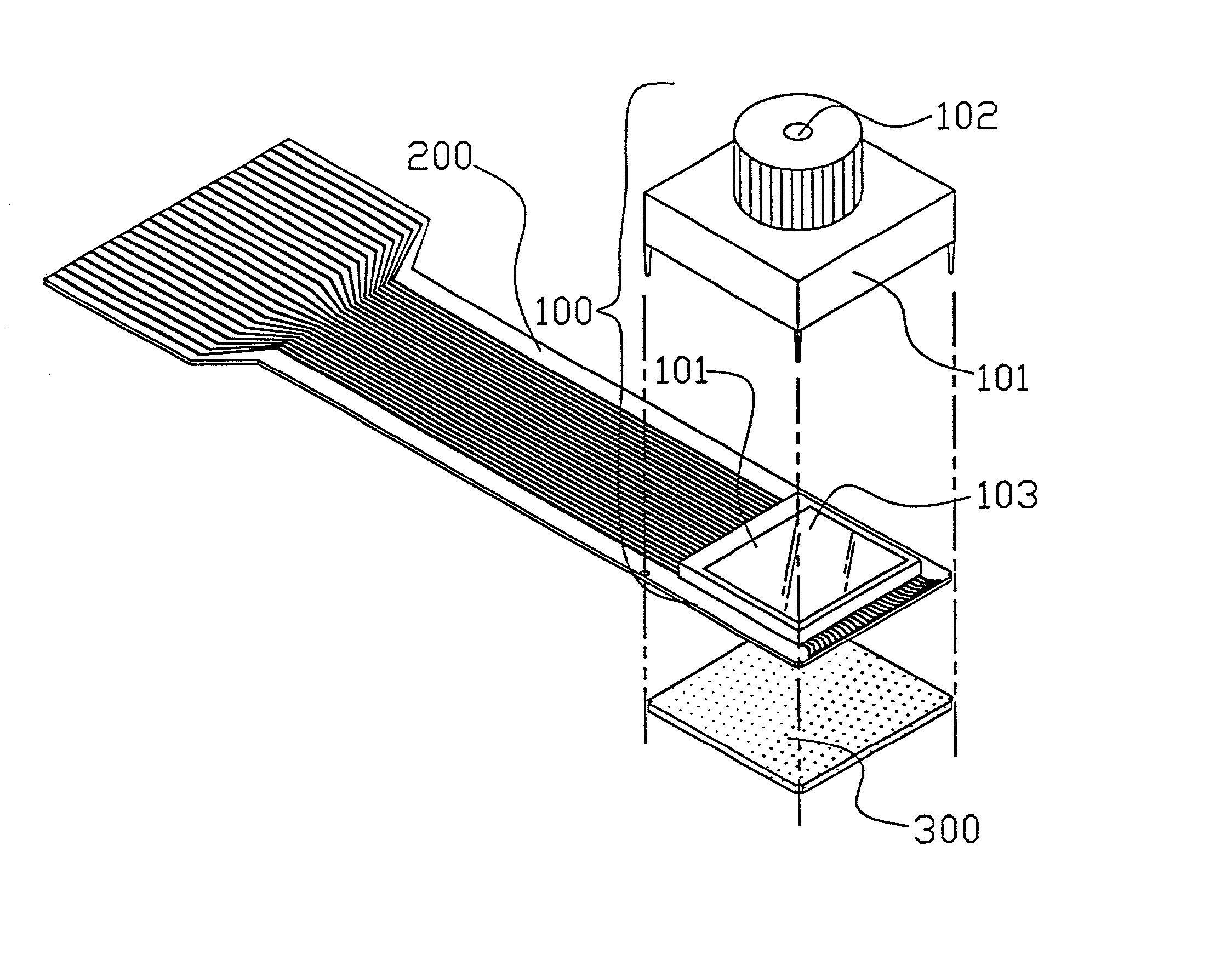
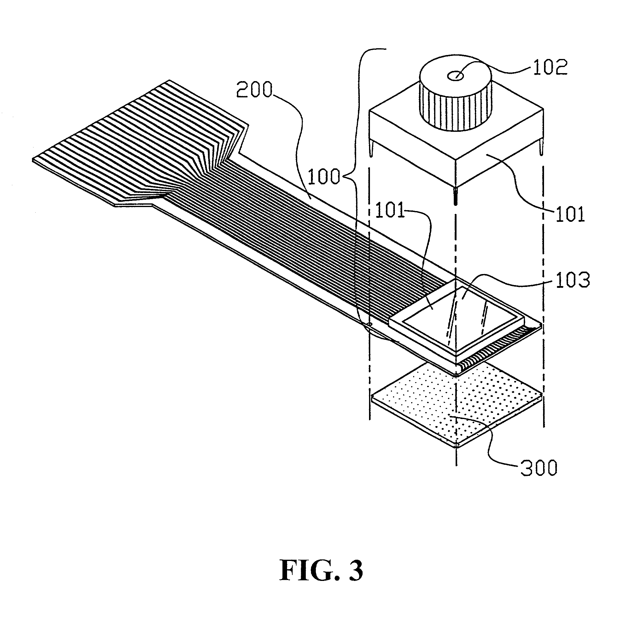
[0019] FIG. 2 is a perspective view showing an improved structure of the chip package implemented on a digital photographic lens device. As shown in the figure, the present improved structure of the chip package can be used in digital photographic lens device with hidden chip connected to transmission lines. The digital photographic lens device has a lens device assembly 100, a flexible circuit board 200 and a hard thin plate 3...


PUM


Abstract

An improved structure of a chip package is disclosed. The improved structure of a chip package for used in the package structure of a digital photographic lens device with hidden chip connected with transmission lines, characterized in that the improved structure comprises a sectional of flexible circuit board and a hard thin board and the mounting legs of the photographic lens device assembly are mounted onto the flexible photographic lens device assembly having corresponding electrically connection points, and the flexible circuit board is connected to the back panel of the digital photographic lens device and is mounted with the hard thin plate.

Description

[0001] (a) Field of the Invention[0002] The present invention relates to an improved structure of a chip package, and in particular, a package structure with chip used in digital photographic lens device connected with a plurality of transmission lines. Flexible circuit board is employed directly as transmission lines for the photographic lens device.[0003] (b) Description of the Prior Art[0004] FIG. 1 is a conventional package structure with chips for a digital photographic lens device connected with transmission lines. As shown in FIG. 1, the connection legs at the base housing 10 of a photographic lens device 1 are first mounted onto a hard base seat 20 (being fabricated from a ceramic or PC board material). The surrounding of the base seat 20 is provided with a plurality of lines 21 connected to the connection legs of the chip 11. The hard base seat 20 is soldered to other layout transmission lines or other hard circuit board with electronic components of related functions. Afte...

Claims


Application Information

Patent Timeline
IPC IPC(8): H04N5/225
CPCH04N5/2253H04N23/54
Inventor TING, CHIH-YU
Owner OPCOM
Why Eureka
Try Eureka