Method of processing a semiconductor wafer and substrate for semiconductor wafers used in the same

a technology of semiconductor wafers and substrates, applied in the direction of layered products, chemistry apparatus and processes, synthetic resin layered products, etc., can solve the problems of difficult to grind the semiconductor wafer without damaging, the stiffness of the semiconductor wafer becomes very low, and the access is interrupted

Inactive Publication Date: 2003-06-05
DISCO CORP
View PDF9 Cites 1 Cited by
  • Summary
  • Abstract
  • Description
  • Claims
  • Application Information

AI Technical Summary

Benefits of technology

[0007] It is the second object of the present invention to provide a substrate which can be advantageously used as a substrate to be stuck on the front surface of a semiconductor wafer to support the semiconductor wafer and can prevent the semiconductor wafer from being damaged without fail when it is removed from the front surface of the semiconductor wafer, in the method of processing a semiconductor wafer which attains the first object.
[0012] a grinding step of adsorbing the front surface of the semiconductor wafer to a chuck means through the substrate and grinding the back surface of the semiconductor wafer by applying a grinding means to the back surface of the semiconductor wafer to reduce the thickness of the semiconductor wafer;

Problems solved by technology

For instance, when the thickness of a silicon semiconductor wafer is greatly reduced, the stiffness of the semiconductor wafer becomes very low, thereby making it difficult to grind the semiconductor wafer without damaging it and to carry the ground semiconductor wafer at a predetermined speed.
However, this access is interrupted by the protective substrate or protective tape.

Method used


Image

  • Method of processing a semiconductor wafer and substrate for semiconductor wafers used in the same
  • Method of processing a semiconductor wafer and substrate for semiconductor wafers used in the same
  • Method of processing a semiconductor wafer and substrate for semiconductor wafers used in the same

Examples


Embodiment Construction

of the semiconductor wafer processing method and the substrate used in the method of the present invention will be described in detail with reference to the accompanying drawings.

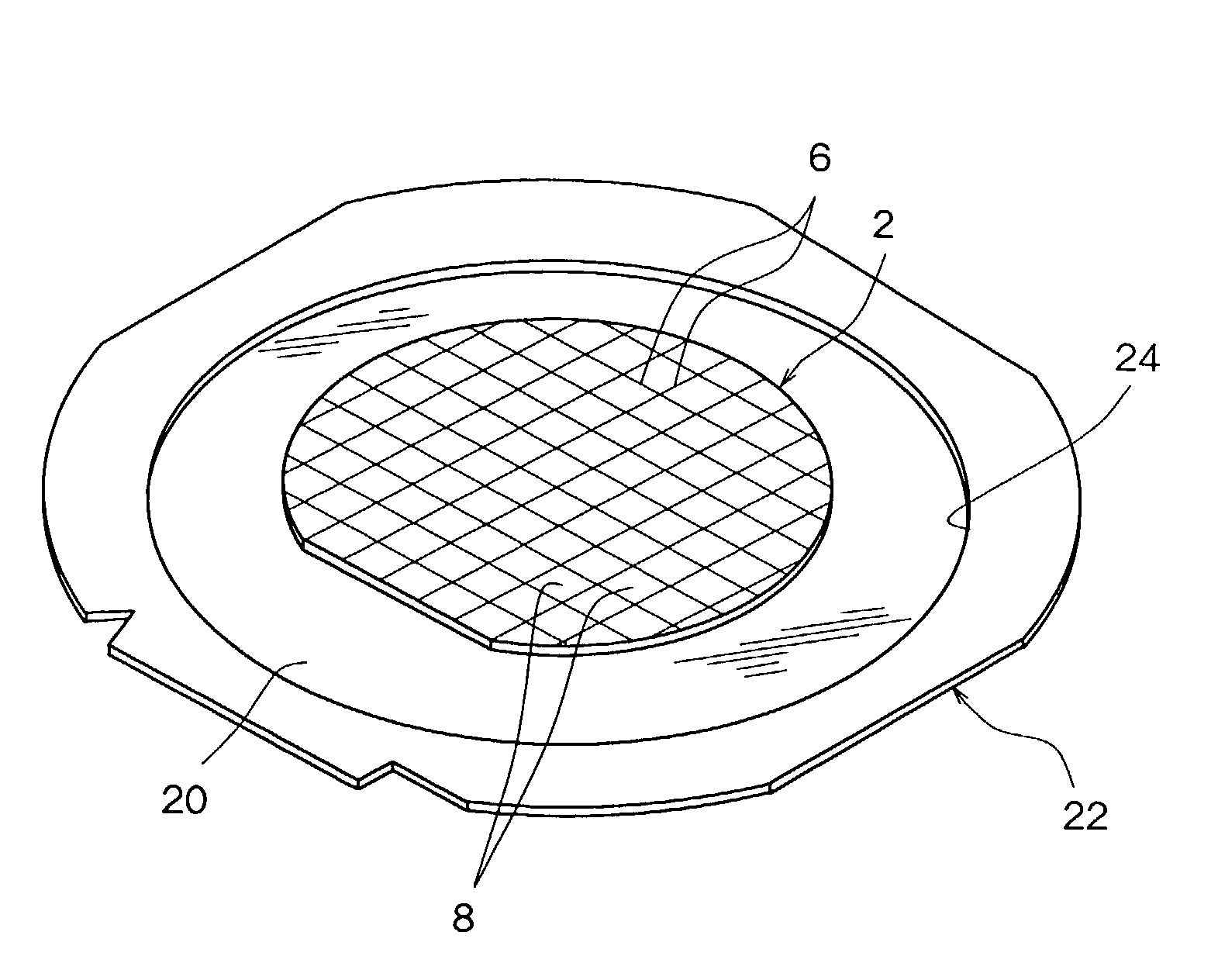
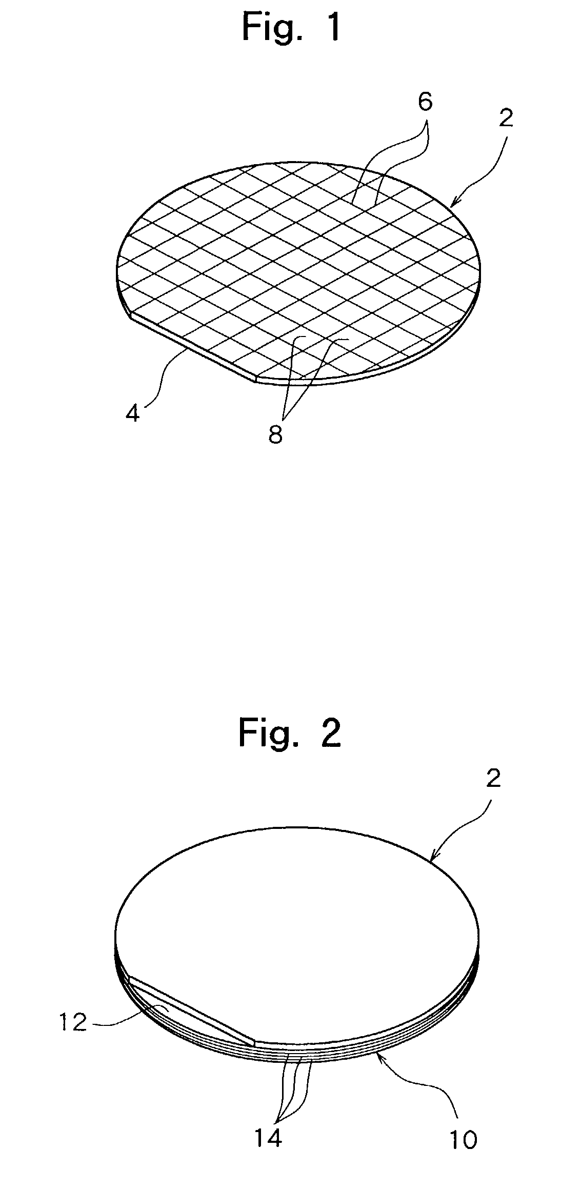
[0026] FIG. 1 shows a typical example of a semiconductor wafer to which the processing method of the present invention can be applied. The illustrated semiconductor wafer 2 has a shape like a disk having a linear edge 4 called "orientation flat" in part of its periphery and has a large number of rectangular areas 8 defined by streets 6 arranged in a lattice form in its front surface. A semiconductor circuit is formed in each of the rectangular areas.

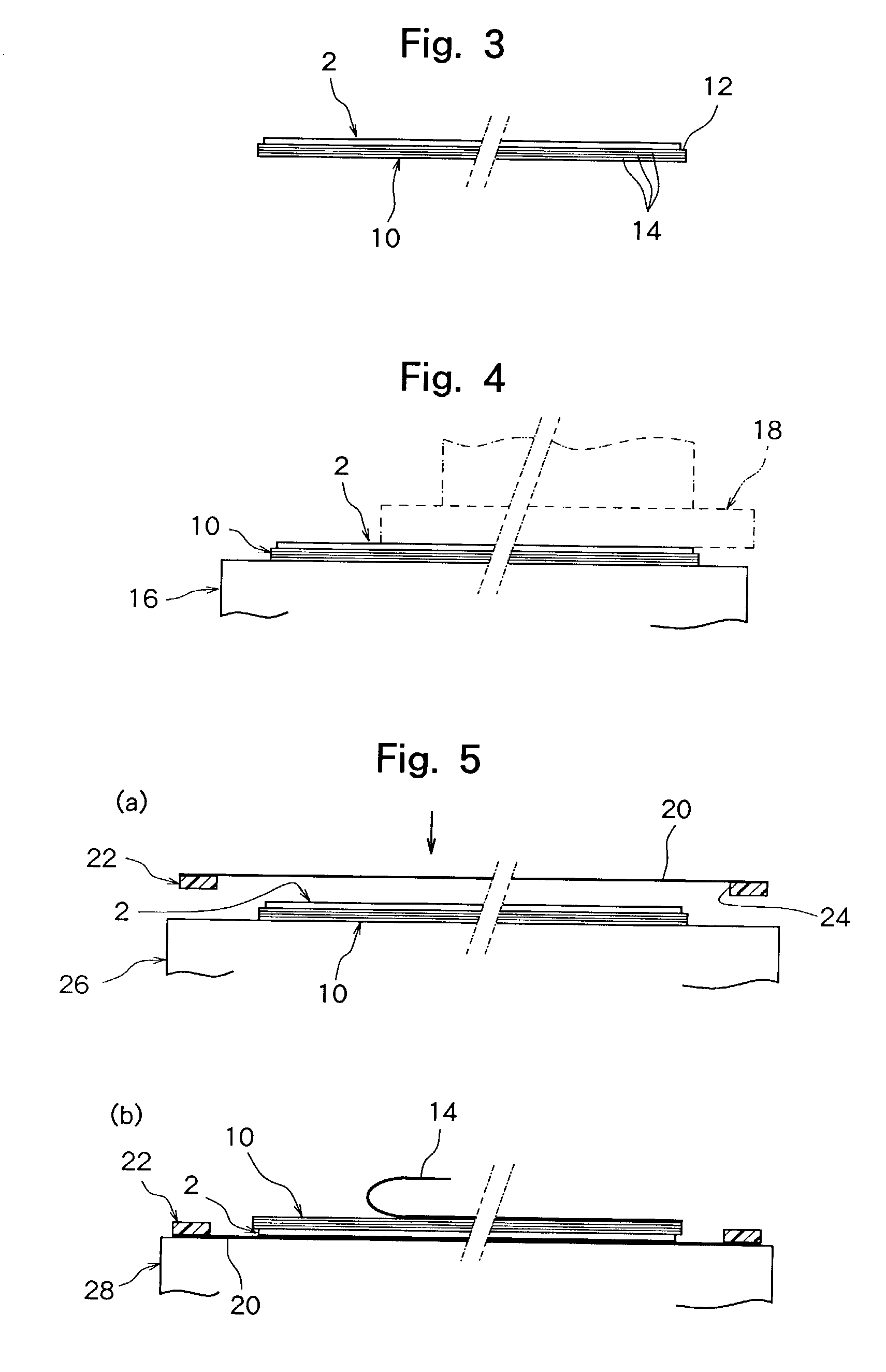
[0027] A mounting step is carried out in the processing method of the present invention. In this mounting step, as shown in FIG. 2 and FIG. 3, the semiconductor wafer 2 is mounted on a substrate 10 by sticking the front surface of the semiconductor wafer 2 on the substrate 10. The substrate 10 may have a disk-like shape or a shape similar in shape to the semicon...


PUM

PropertyMeasurementUnit
thicknessaaaaaaaaaa
thicknessaaaaaaaaaa
lengthaaaaaaaaaa

Abstract

Prior to a grinding step, the front surface of a semiconductor wafer is stuck on a substrate to be mounted on the substrate. The transfer step of mounting the semiconductor wafer on a frame having a mounting opening in its center portion through a mounting tape and removing the substrate from the front surface of the semiconductor wafer is carried out between the grinding step and the subsequent treating step. The substrate is formed of a laminate consisting of a plurality of layers.

Description

[0001] The present invention relates to a method of processing a semiconductor wafer having a large number of rectangular areas defined by streets arranged in a lattice form in its front surface and having a semiconductor circuit in the respective rectangular areas, and to a substrate used in this processing method.DESCRIPTION OF THE PRIOR ART[0002] As is known to people of ordinary skill in the art, in the production of a semiconductor device, a large number of rectangular areas are defined by streets arranged in a lattice form in the front surface of a semiconductor wafer, and a semiconductor circuit is formed in each of the rectangular areas. The back surface of the semiconductor wafer is ground to reduce its thickness and the semiconductor wafer is cut along the streets to separate the rectangular areas from one another, thereby forming semiconductor chips.[0003] In general, a grinding means is applied to the back surface of the semiconductor wafer to reduce its thickness to a p...

Claims


Application Information

Patent Timeline
Patent Type & Authority Applications(United States)
IPC IPC(8): B32B27/08H01L21/00H01L21/301H01L21/68
CPCB32B27/08H01L21/67132H01L21/6835H01L2221/6834H01L2221/68327H01L2221/68336H01L21/6836H01L21/00
Inventor NANJO, MASATOSHI
Owner DISCO CORP
Why Eureka
Try Eureka